

For product requests contact us by using the
- Contact formular,
- Email (sales@suragus.com) or
- Phone (+49 351 32 111 520).
Functional thin films on glass, foil and wafer are crucial to many applications and industries. Modern coatings are adapted to meet the growing demand and requirements such as:
In order to achieve these goals, SURAGUS offers inline and offline testing technology.
Application overviews are available for the following industries:
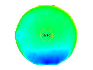
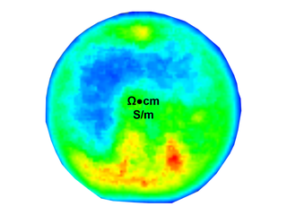
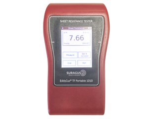
The sheet resistance, describes the ability of a square layer to conduct a certain current. This characteristic is the most important quality parameter for surface electrodes and is determined during layer deposition or for quality assurance of conductive thin films. The sheet resistance is specified in ohms / sq or OPS, in order to achieve a differentiation for the specific resistance, which is indicate in ohms.
Conductive functional layers are used in various industries. Common materials are:
| Transparent electrodes | Metallic Electrodes |
|---|---|
|
|
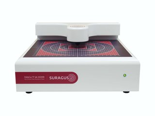
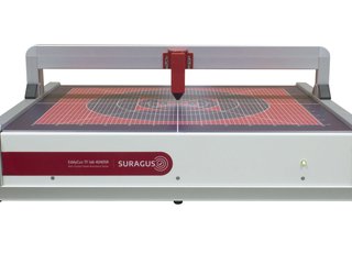
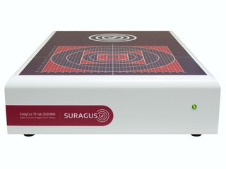
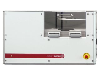
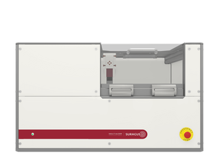
SURAGUS provides with the EddyCus TF series quality assurance systems for the determination of the electrical conductivity. Therefore, the non-contact eddy current technology is being used to measure sensitive or encapsulated layers. The testing is automated and can be adapted individually according to customer requirements.
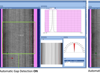
Spatially resolved eddy current testing or eddy current impedance spectroscopy can be used to analyse the homogeneity of resistive and dielectric properties. Additionally, conductivity variations can also be utilized to allocate defects and material or process related information.


The eddy current method is particularly sensitive for effects that disrupt the induced current flow laterally.
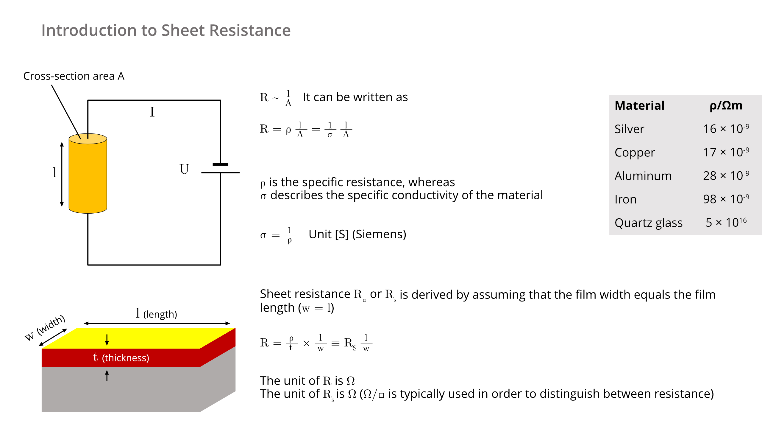
The optical transparency describes the ability of light of a certain wavelength (typically in the visible region) to penetrate a certain layer, without being reflected, absorbed or scattered. It is measured in% of the intensity of the incident light on the layer.
Another possibility to describe the optical transparency (OT) is the optical density (OD), which can be calculated by using the following formula: OD = -log_10OT
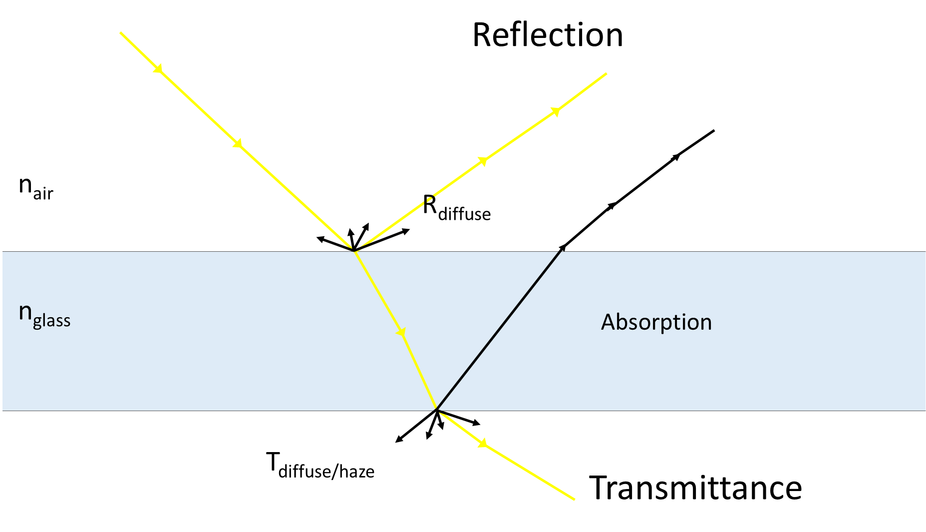
The quality of a transparent electrode, is described by its electrical and optical properties. Therefore, for the development and quality assurance of transparent conductive layers always both parameters are important. The technological trend is towards ever more conductive layers with very high optical transparency.
Since both variables often have to be measured and the measurement by using several measuring systems is time-consuming, capital and space intensive, EddyCus hybrid series was developed as a universal testing system.
Many types of functional layers must be transparent to visible light:
The technological trend is towards ever more conductive layers with very high optical transparency.
The contactless measuring sheet resistance measurement devices from SURAGUS can be equipped with an additional sensor for measuring the light transmittance at a single wavelength or spectral measurement units. These combined hybrid measurement devices enable the quick and easy measurement of the sheet resistance and optical transparency.
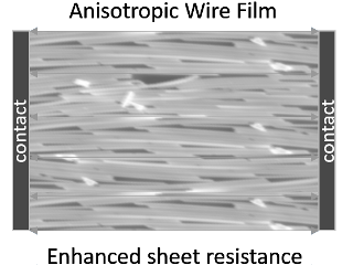
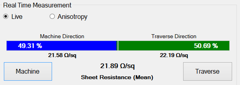
The sheet resistivity anisotropy describes a change in the sheet resistance of a thin layer depending on the direction of the current flow. The anisotropy of the sheet resistance is based directly on an electrical anisotropy the conductive thin film.
For example, the conductivity of a layer of uniformly oriented nanowires be very high in the longitudinal direction of the wires, but much lower perpendicular to it.
Electric anisotropic layers are extremely interesting as they guarantee a certain conductivity in a desired preferential direction and maintain at the same time by using less material, a high optical transparency of the layer.
SURAGUS manufactures and sells versatile, non-contact testing equipment for electrical anisotropy and optical transparency.
The non-contact measurement of the sheet resistivity anisotropy provides an accurate and in-depth analysis of the direction, characteristics and quality of electrical anisotropy.
The derived results allow an extended analysis of the production process, fast process control and reliable quality assurance.
The measurement of electrical anisotropy is relevant where the high conductivity of a thin film is to be ensured in a certain direction and should remain a high optical transparencey of the layer.
This is especially important for:
SURAGUS manufactures and sells versatile, contactless testing equipment for electrical anisotropy.
The non-contact measurement of the sheet resistivity anisotropy provides an accurate and in-depth analysis of the direction, characterization and quality of electrical anisotropy.
The derived results allow an extended analysis of the production process, fast process control and reliable quality assurance.
For product requests contact us by using the