How to Select a Layer Thickness Measurement Technology
Layer Thickness Measurement Technologies
Clustering of technology
- Direct vs. indirect methods
- Destructive vs. non-destructive methods
- Often destructive methods allow the direct measurement whereas most non-destructive (non-contact) methods use indirect relations and, therefore, require calibration or reference parameters.
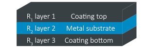
Considering material stack e.g. substrate separation
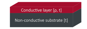
- Conductive and non-conductive
- Transparent and semi- or non-transparent
- Reflective and non-reflective
- Ferromagnetic and non-ferromagnetic
Challenges of Layer Thickness Measurement
Challenges of metal layer thickness measurement involve:
- Multi-layer-thickness measurement
- Ultra-thin layer thickness measurement
- Boundary layer thickness measurement
Thickness measurements can often be performed using different techniques. Typically, there are many influencing variables from substrates and layer properties to environment and measurement type which should be taken into close consideration.
Layer Thickness Sensors
Thickness sensors differentiate materials using various technologies. Common techniques involve surface profilers, ellipsometry, dual polarization interferometry and scanning electron microscopy to analyze the cross-sections of the samples.
Thickness Gauging Methods
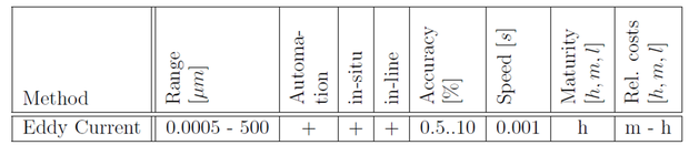
The data displayed in the following comparison tables is obtained from "Nitzsche, K.: Schichtmeßtechnik. Vogel, 1997."
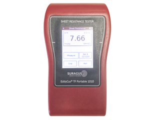
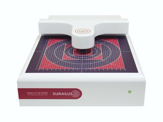
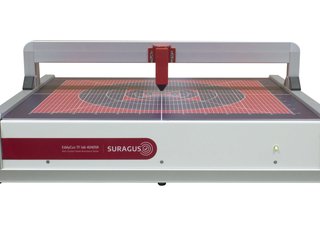
Eddy Current Thickness Gauging Methods
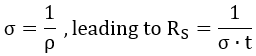
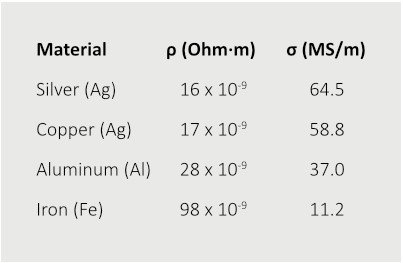
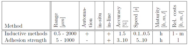
Eddy current measurement is a reliable non-contact testing method. It is applicable to a wide range of different tasks, such as detection of surface damages, vibration and deformation measurement, measurement of material properties like electrical conductivity and magnetic permeability as well as proximity sensing. Proximity sensing and sensing of conductivity allows for a very precise determination of the thickness of various layer/substrate systems.
- Requires conductive coating
- Very large measurement range
- Fast measurement method
- Mature method
- Medium to high costs
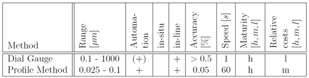
Mechanical Thickness Gauging Methods
Dial gauges and comparator gauges are relatively simple tools which play a subordinate role. A tip scans the surface using the power of gravity or of a spring and then converts the jump of the tip at a step into the thickness. Similar methods are profile methods that are primarily used for roughness investigations. A diamond tip scans the surface and converts the movement into an amplified electrical signal. Advantages of those methods are that they are direct measurement methods with great reproducibility.
They are inexpensive, there are no requirements towards the layer system and roughness can be erased by averaging. The main disadvantage is the need for a step and the contact to the layer that may cause elastic or plastic deformation. Moreover, they are not applicable for in-situ measurements.
- Typically requires physical contact and a physical step
- Well known technology
- Inexpensive
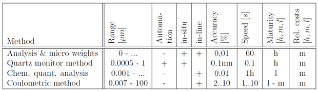
Thickness Determination by Weight Measuring
Knowing the layer area and the density of the layer material allows the determination of thickness by weight measuring. This is achieved either by measuring the weight difference of the structure of interest or by investigating the weight of a reference structure. Analysis and micro scales or other special disposition weight measuring methods are very precise, but allow very low loads and an in-situ application is difficult. A common and even more precise and in-situ applicable method is the quartz monitor method. A quartz in the chamber next to the substrate is coated under the same condition. The quartz alters its oscillation characteristics depending on its weight which is monitored and evaluated. It is an extremely precise method that is also suitable for coating sequences. Another approach is the weight measurement of the consumed vapored material. It is a simple but not very precise method. Furthermore, there are also chemical quantitative analysis which determines thickness by measuring the duration of a chemical reaction for detachment of the layer. The coulometric method determines the thickness in a reverse electrolysis by measuring the changing potential. It is very precise but destroys the layer so it is mainly used for lab applications.
- Medium costs
- Inline and insitu applications
- Mature technology
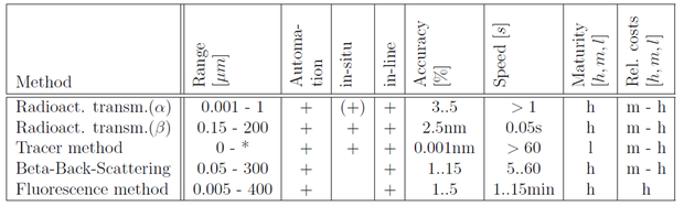
Radiometrical Thickness Gauging Methods
The interaction of ionized or radioactive emission with layer matter provides plenty of information on material characteristics. Depending on material and thickness, different emission types are applied. Commonly used are alpha, beta, gamma, X-ray or electron emission. Effects are transmission, absorption and back scattering. All approaches use a source and a receiver. Common receivers are ionization chambers, radiation counters, scintillator counters or crystal counters. A high emission supports a high resolution but increases hazardous radiation. The radioactive transmission approach analyzes, similar to the optical transmission approach, the weakening intensity caused by the sample. An essential condition is that the proportion of absorption due to the substrate is not too high so that variations due to the layer can still be analyzed. Furthermore, a calibration curve is required and both sides of the sample are occupied for measurements. The Tracer method mixes radioactive isotopes into the layer and determines the thickness by the radiation intensity. In the Beta-Back-Scattering method a sample is bombarded with a tilted collimated beam of electrons from a weak radioactive beta source. As reflected primary radiation is blocked by an obstacle, only radiation emitted by the layer is received and then referenced to the thickness. Another well established approach is the Fluorescence method. Here, electric transitions caused by x-ray, gamma or beta radiation in the atomic shell emit light which is characteristic for every chemical element. Hence, next to thickness gauging also qualitative characterizations are possible. Although all radioactive methods have a high sensitivity, users have to consider potential health issues.
- Variety of testing methods and setups are available
- Mature technology
- Medium to high costs
- Requires safety measure to cope with radioactive tools
Magnetic Thickness Gauging Methods
Magnetometers can be used for all non-ferromagnetic coatings on ferromagnetic substrates. They are often used for rapid quality assurance of galvanic layers (like zinc, copper or aluminum) on steel or iron. Magnetometers evaluate magnetic fields induced by coils that are influenced by the distance to the substrate. Since this technique requires to contact the surface of the test material, it may impact the surface. Despite the simplicity of the approach, there are many issues to consider when contacting a layer as the probe position influences the measurement. Issues are too small samples, non-planar surfaces, roughness and misbalance of the probe. Carried out properly, the method allows thickness determination from few μm to few mm, if referenced to calibration samples. Measurements can be done with various arrangements of one or more coils following the induction law and analyzing various effects. Common are fluxgate magnetometers, rotating coil magnetometers or hall effect magnetometers. In the most basic form, the fluxgate magnetometer comprises two coils which share the same core. In a magnetically neutral background, the input and output currents match but if the core is exposed to a magnetic background field, then the signal changes due to varying saturation efforts. The rotating coil magnetometer induces a sine wave in a rotating coil and evaluates the amplitude of the signal. A hall voltage can be measured when an ashlar conductor or semiconductor is transduced by a current accompanied by a perpendicularly arranged magnetic field. The evaluation of the caused hall voltage provides an insight into the electrical properties, charge carrier density and mobility and, hence, the conductivity. There are many physical effects for consideration but especially for silicon and germanium layers, which have a high hall coefficient, this method allows reliable measurements without the need for references. A further approach is the adhesion strength measurement which analyzes the strength during the detachment of a permanent magnet and converts this into the thickness.
- Mature technologies
- Low to medium high cost
- Require magnetic layers
Optical Thickness Gauging Methods
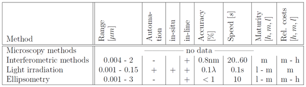
Microscopy methods demand, with a few exceptions, an edge. Thus, a cut into the material is required which can be archived, e.g., by focused ion beam or etching. There are many ways to determine the thickness using microscopy like using depth of focus, scaling with multimeter, light cutting methods or a scan with SEM. Interferometric methods also require a step unless the material is transparent. Interference refers to the interaction of two or more waves that are correlated or coherent with each other.
Interference techniques have been well investigated and developed. Major approaches are transmission interference, incident light interference and interphako interference. Irradiation techniques evaluate the intensity of the perpendicular light beam that is transmitted through the sample. This approach analyzes the reflectance and absorptance behavior of transparent and semitransparent layers. It is a widely applied method for coated foils in the packaging industry. Ellipsometry analyses the change of polarization when parallelized light pervades a transparent or semitransparent layer. Most common is the application in reflection mode. The advantage for in-situ applications is that the area above the sample is not blocked and, hence, a measurement during the coating process is possible. Furthermore, it is an extremely precise, very fast, non-destructive, contact-free and in-situ applicable method which does not require reference measurements. Disadvantageous is the limitation to transparent layers, sensitivity towards micro structural effects, micro roughness and micro criticality.
- Limitation to transparent layers (thin metal layers)
- Sensitivity to micro structural effects and micro roughness
- Suitable for inline application
- Medium to high costs
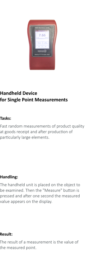
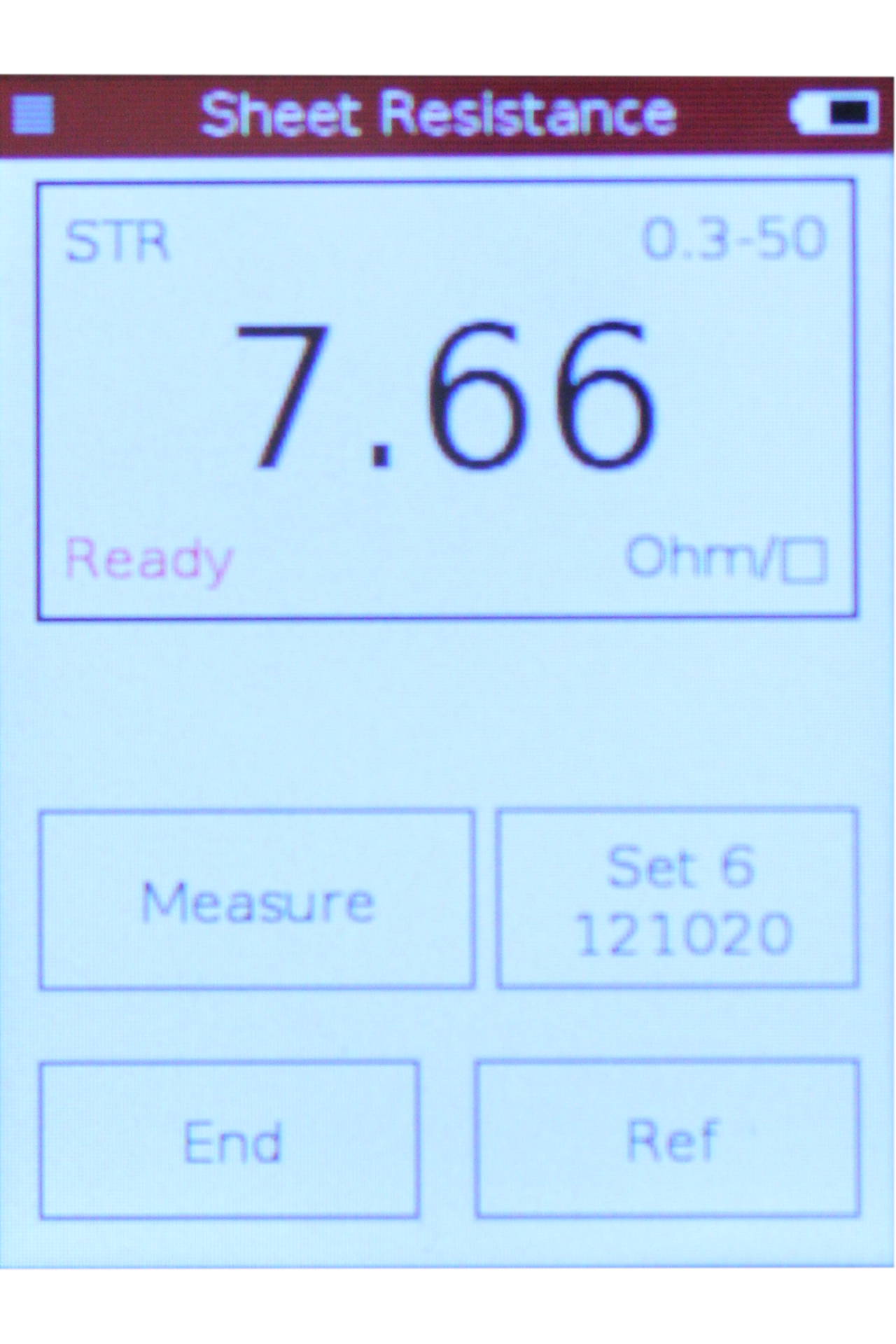
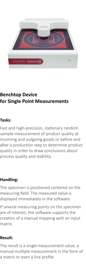
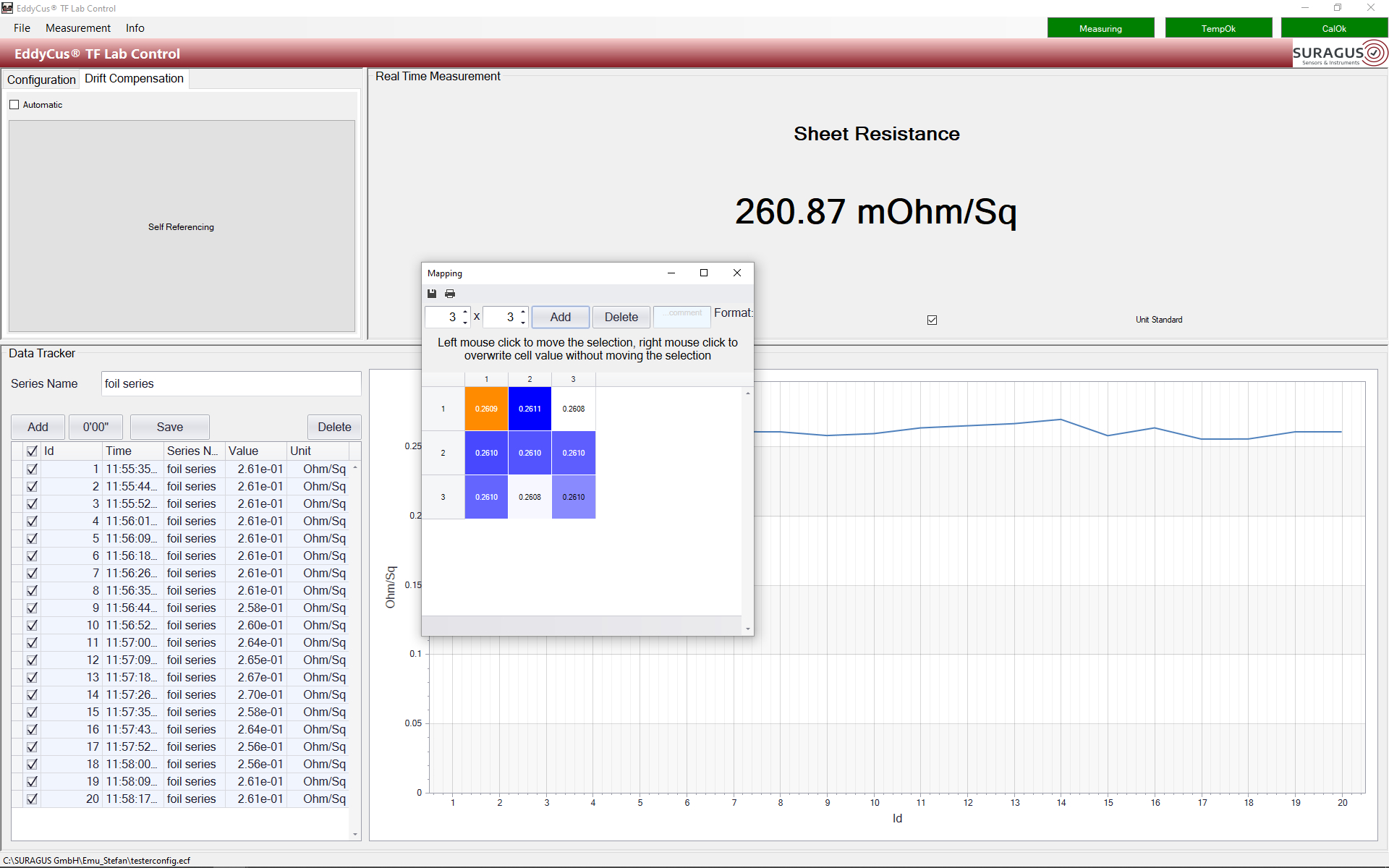
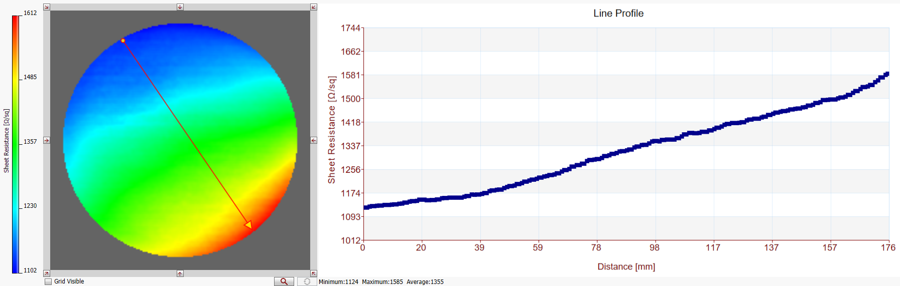
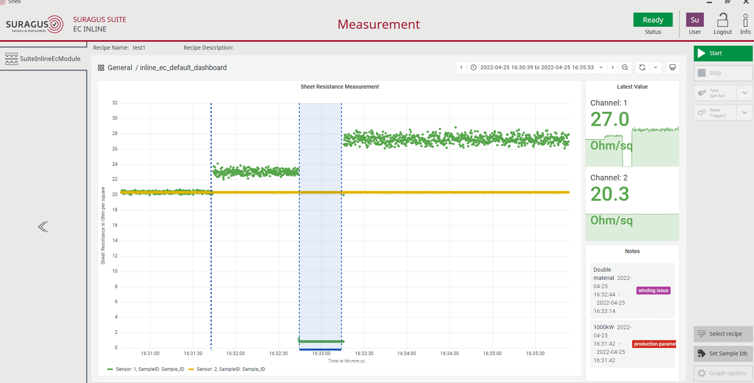
Testing Devices for Metal Layer Thickness Measurements
Industry and R&D laboratories have different requirements when it comes to the number of samples and measurement tasks per day, measurement point density and its automation level. In result, four key testing types are commonly applied:
 layer.")