


For product requests contact us by using the
- Contact formular,
- Email (sales@suragus.com) or
- Phone (+49 351 32 111 520).
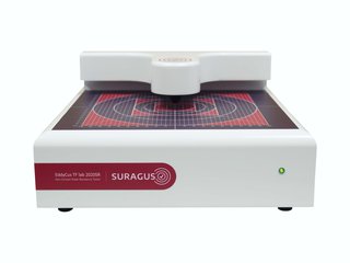
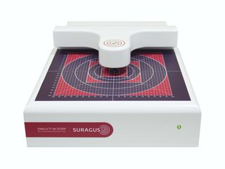
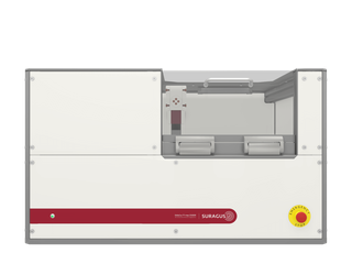
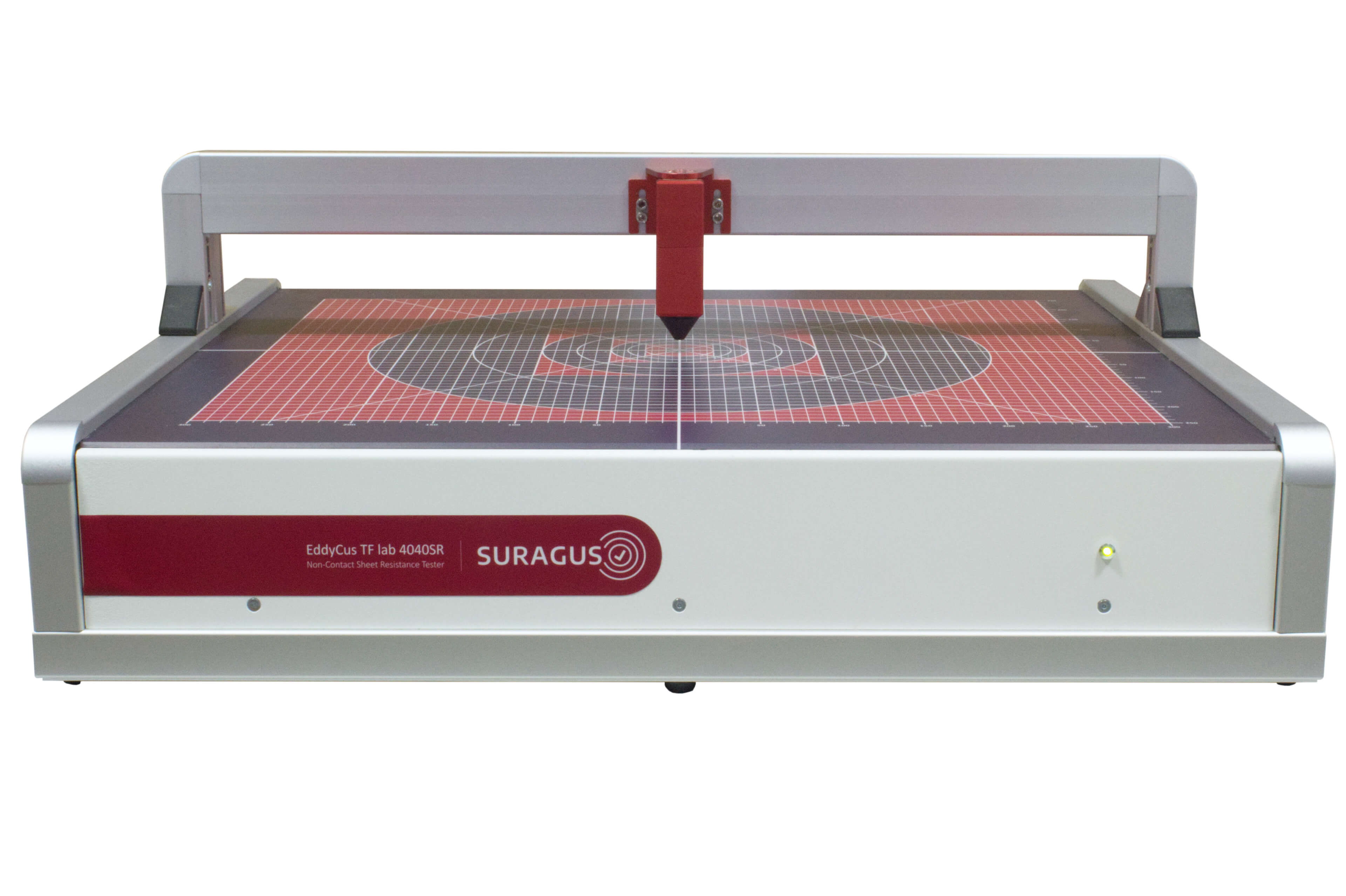
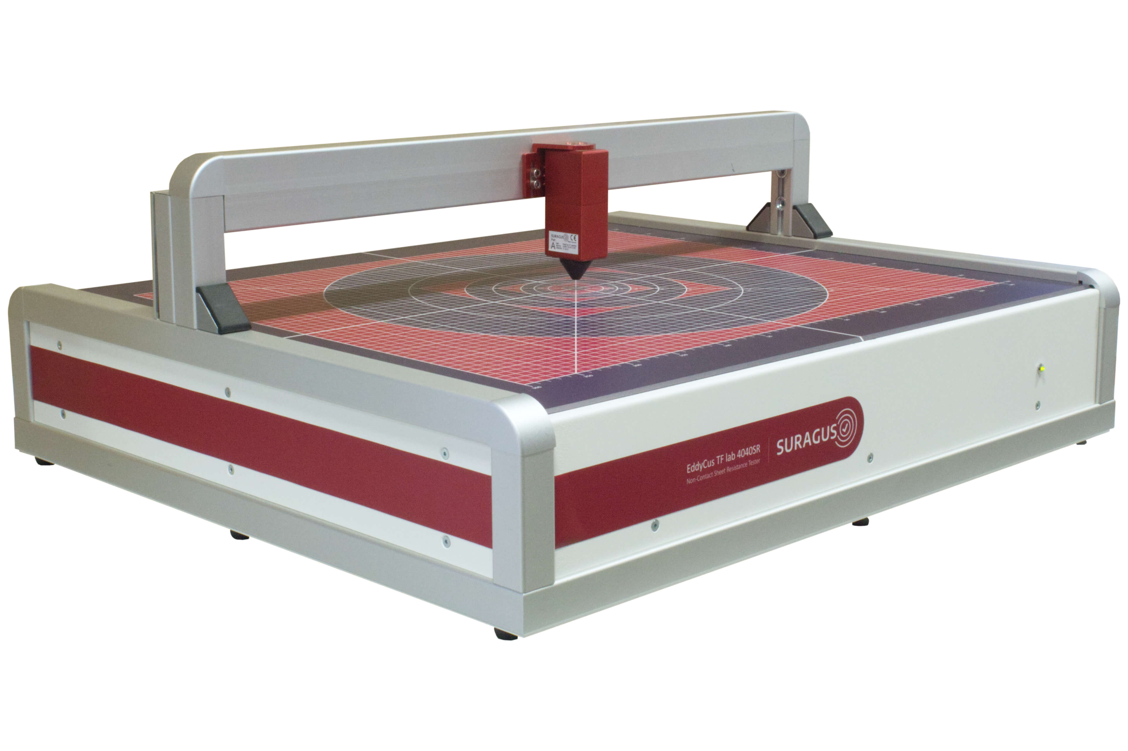
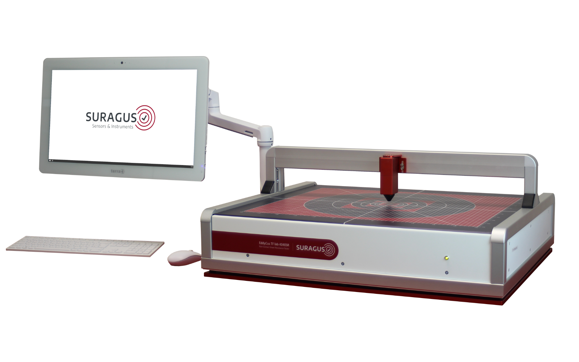
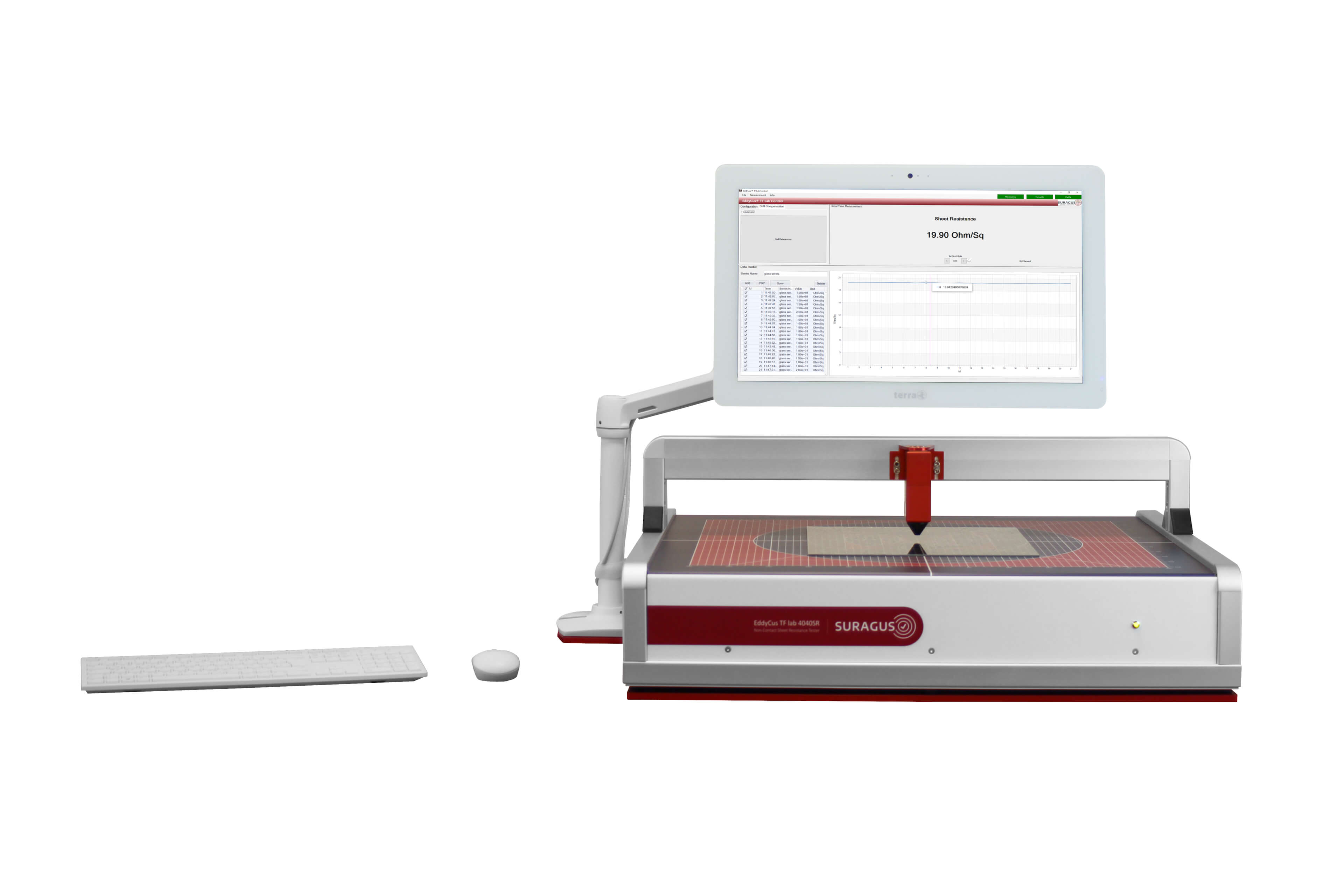
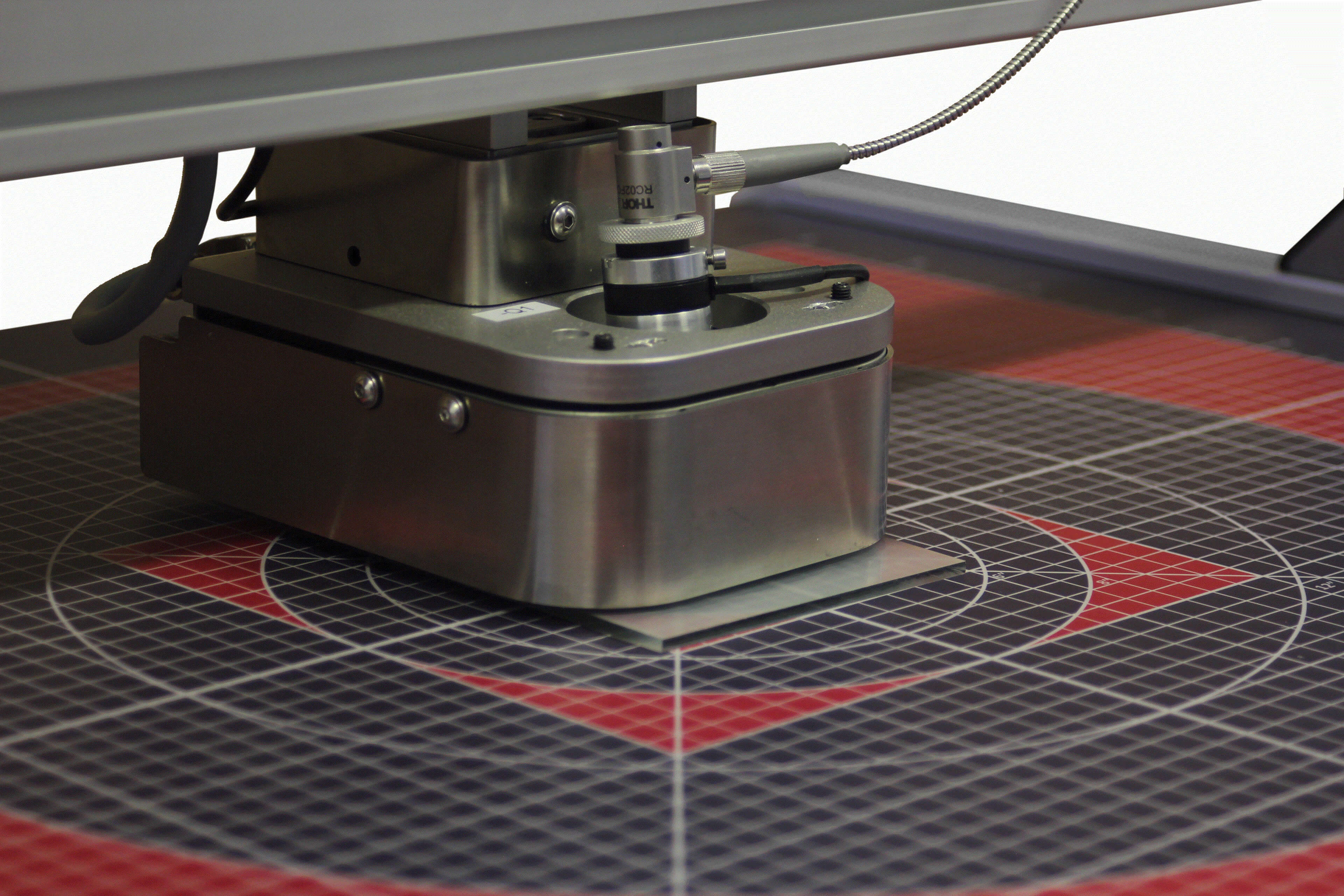
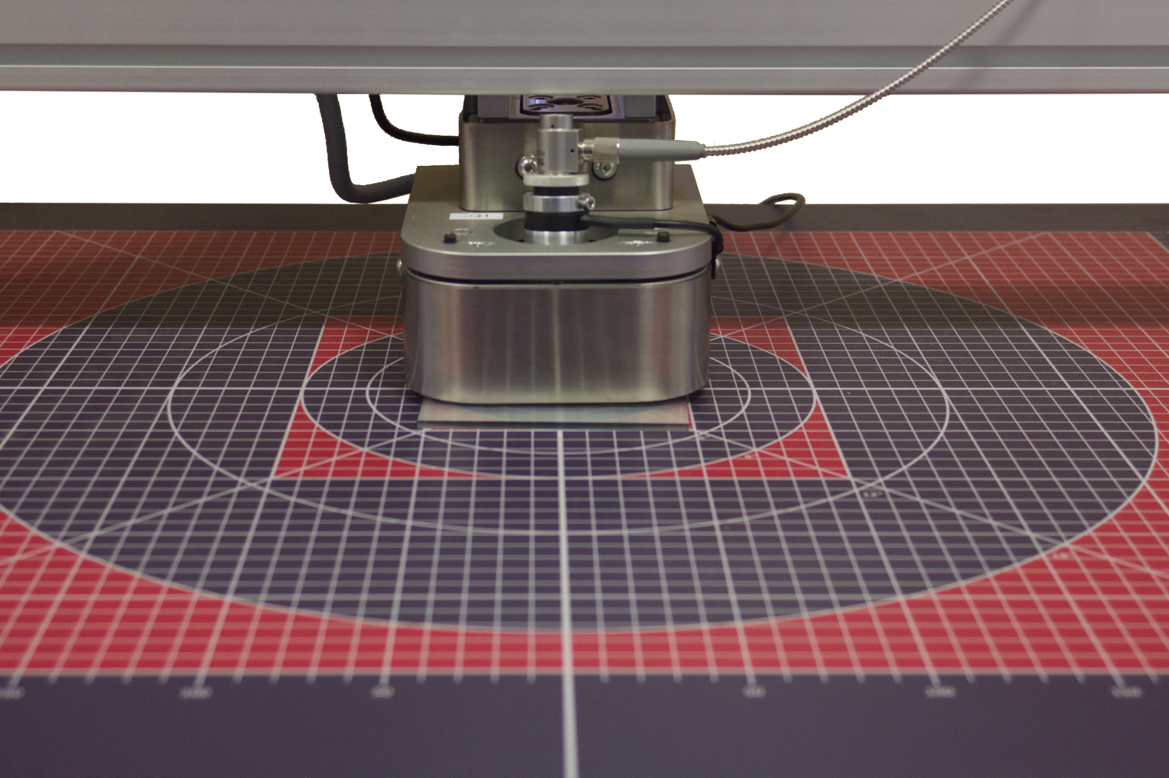
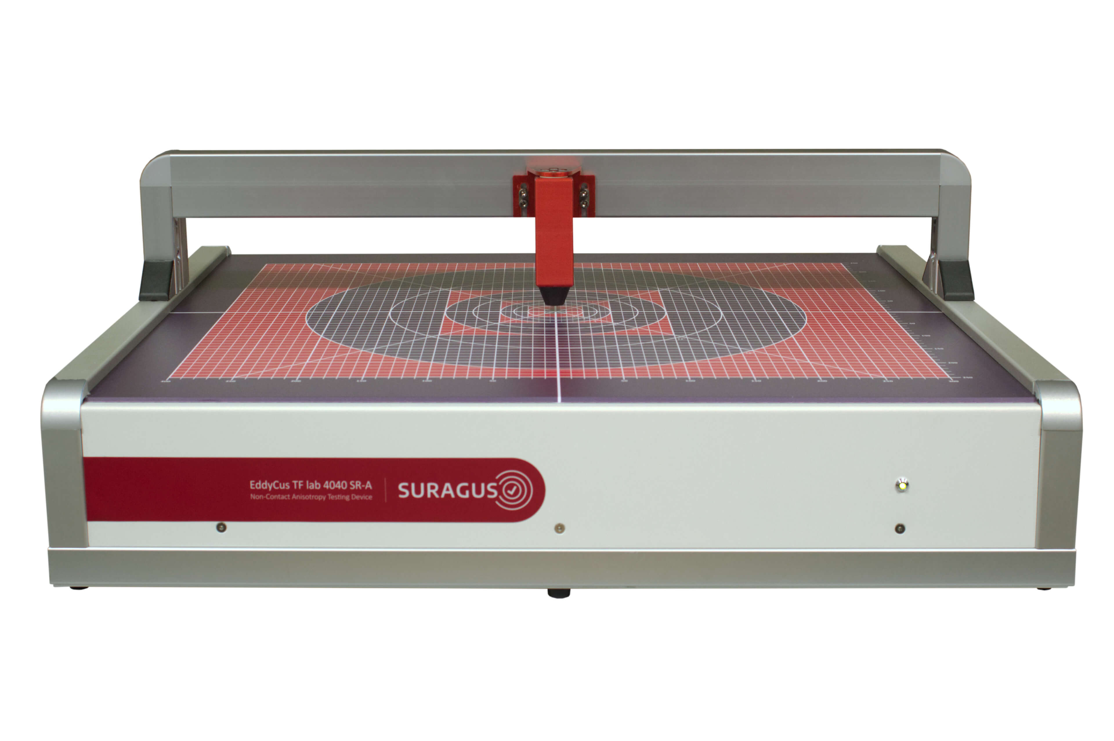
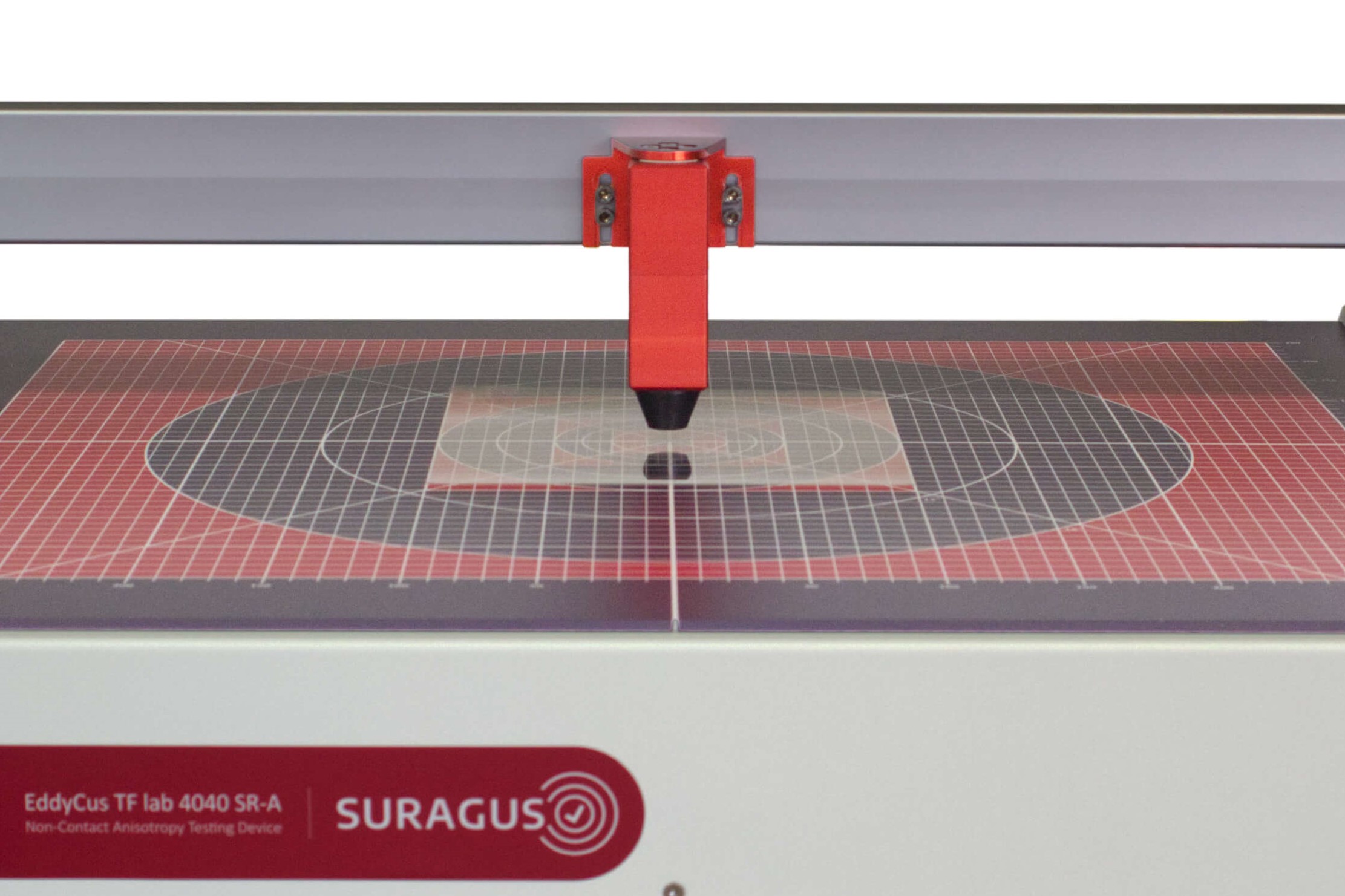
The EddyCus® TF lab 4040 Series is dedicated to non-contact single point measurements on medium sized substrates. The flexibly applicable bench-top device allows depending of its setup the precise manual measurement of sheet resistance, metal thickness, optical transparency or electrical (an)isotropy. Most common applications include the measurement of thin conductive transparent and non-transparent layers, wafers or metal sheets.
The device can be equipped with different sensors including eddy current sensors for electrical characterization or sensors for optical characterization. Variants of the device platform involve the following options.
Combinations of the above are available as well (e.g. 4040SR-MT-T-R-H).
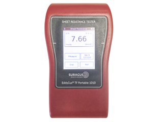
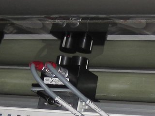
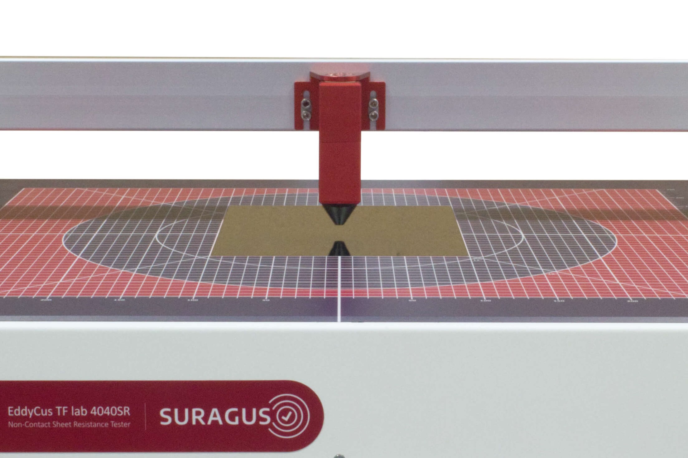
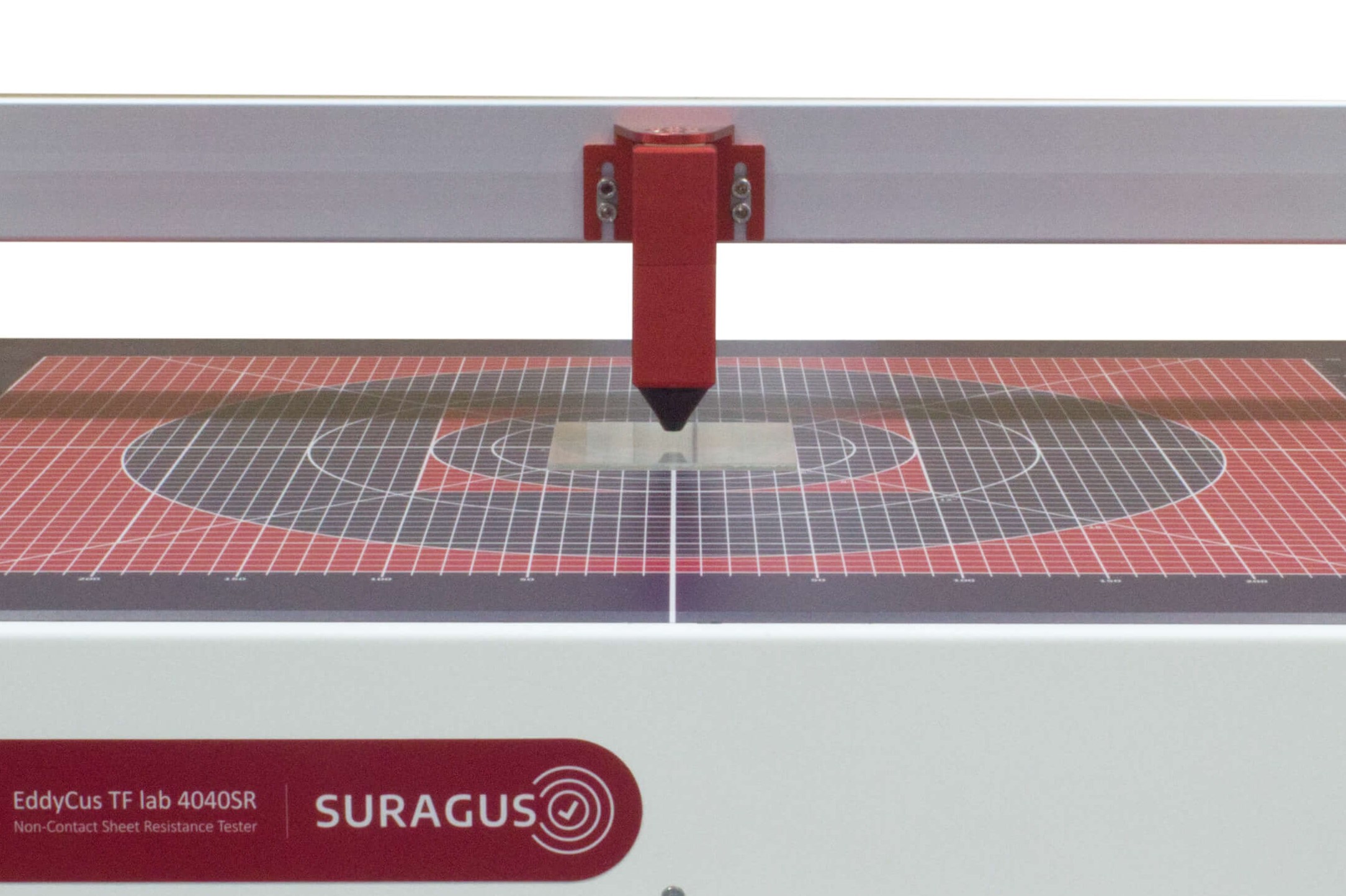
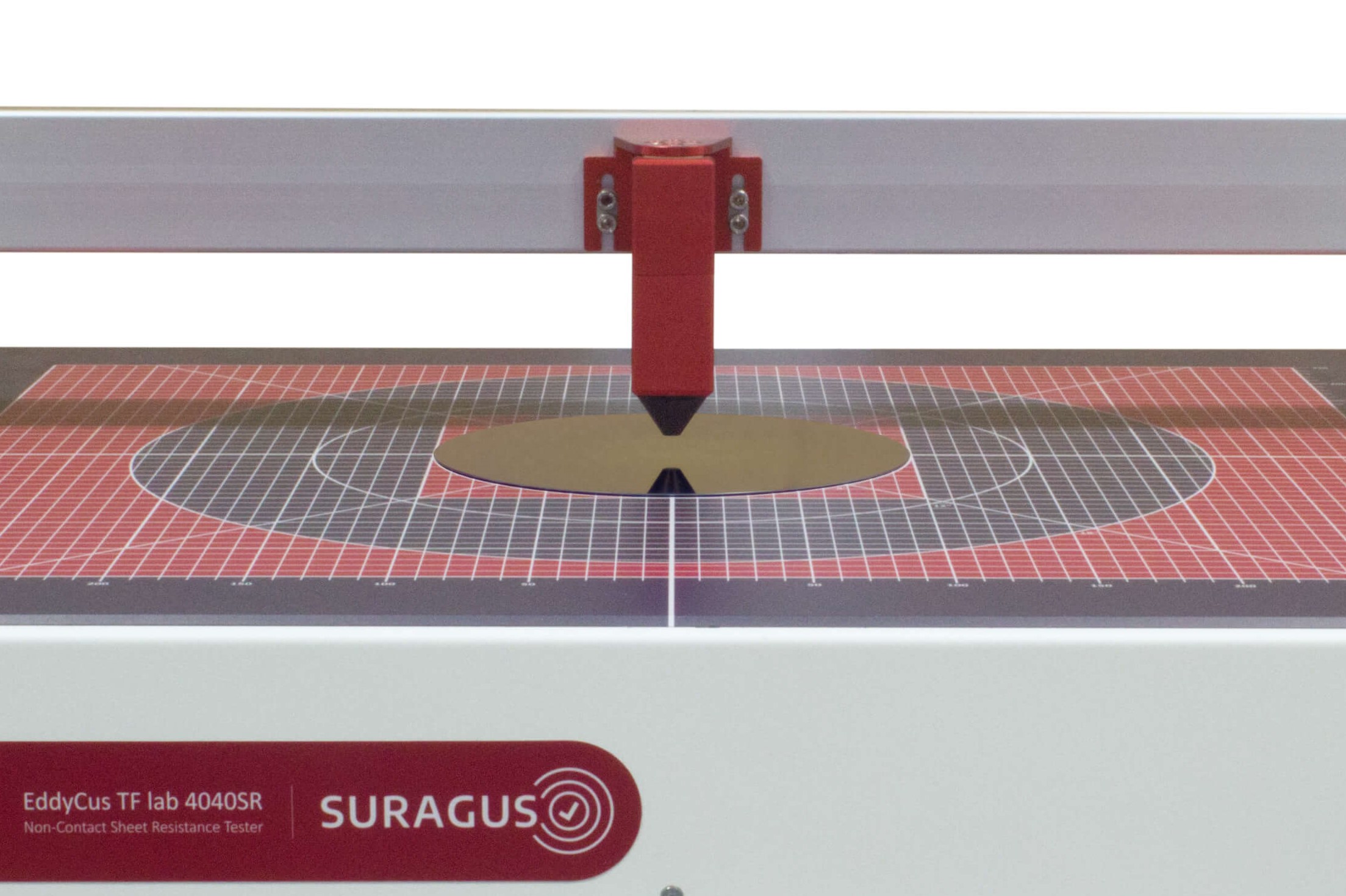
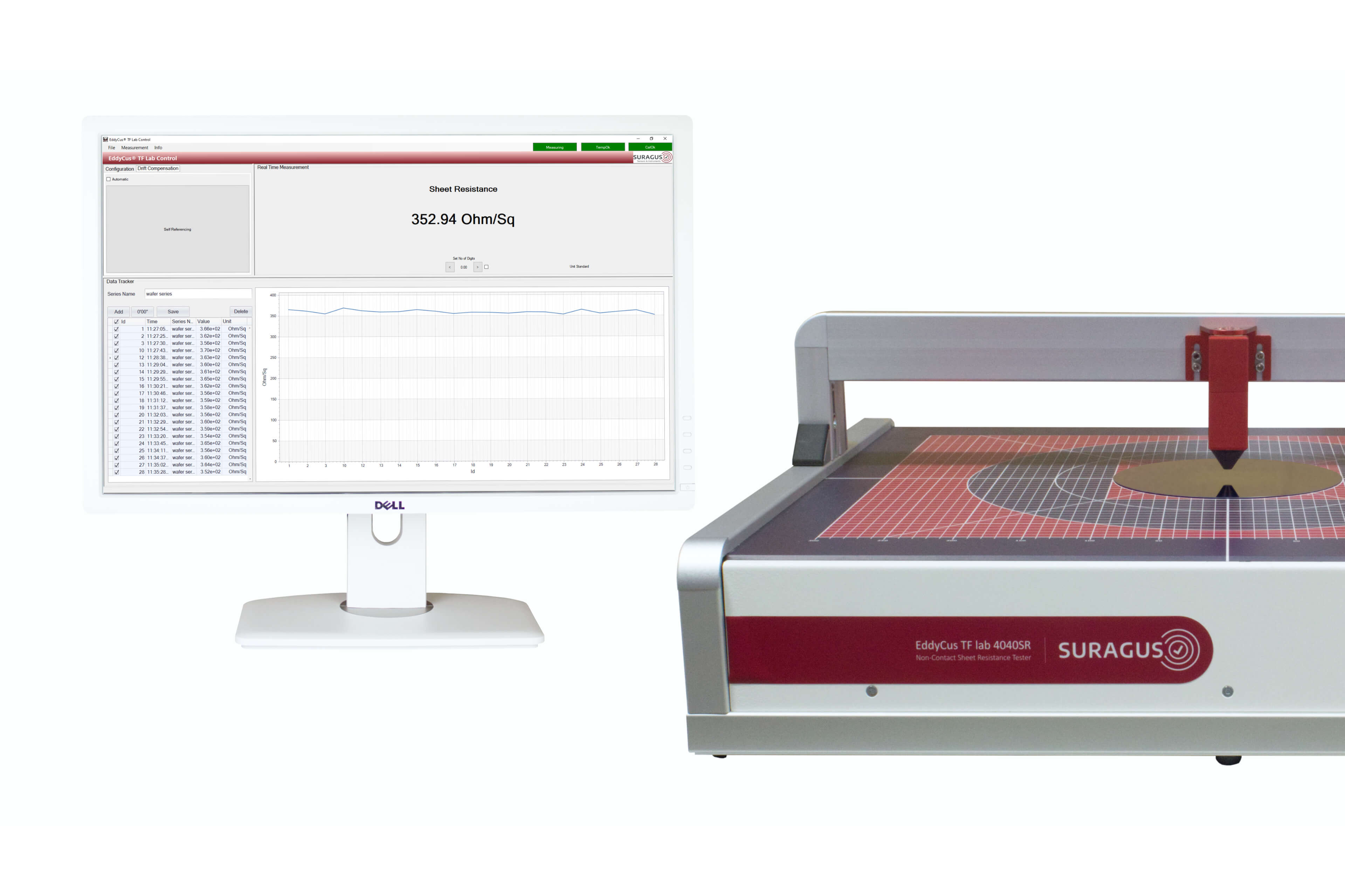
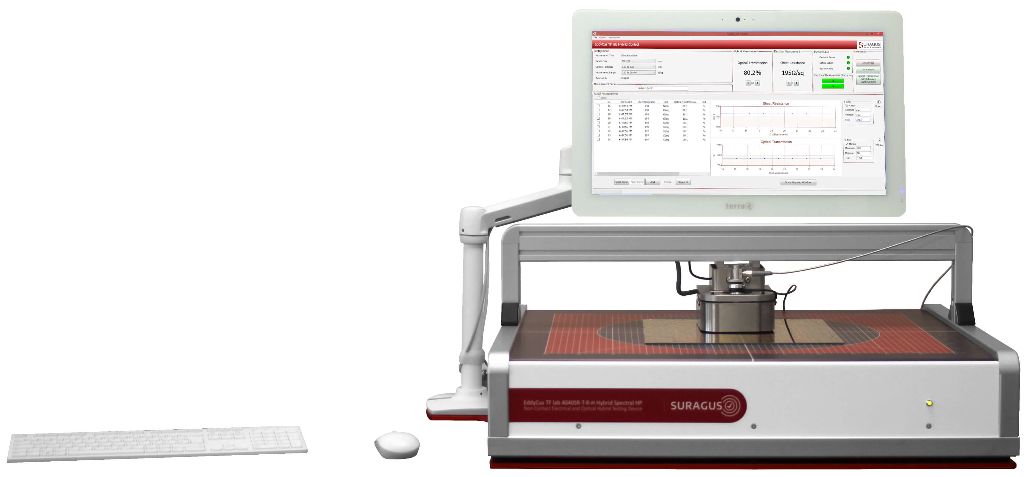
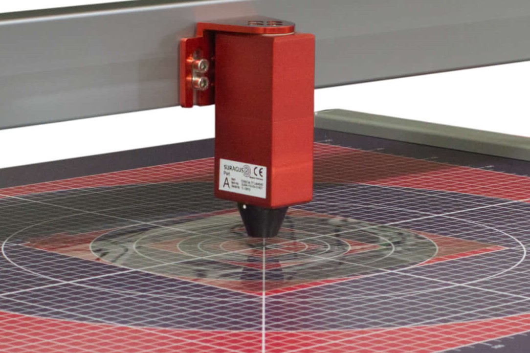
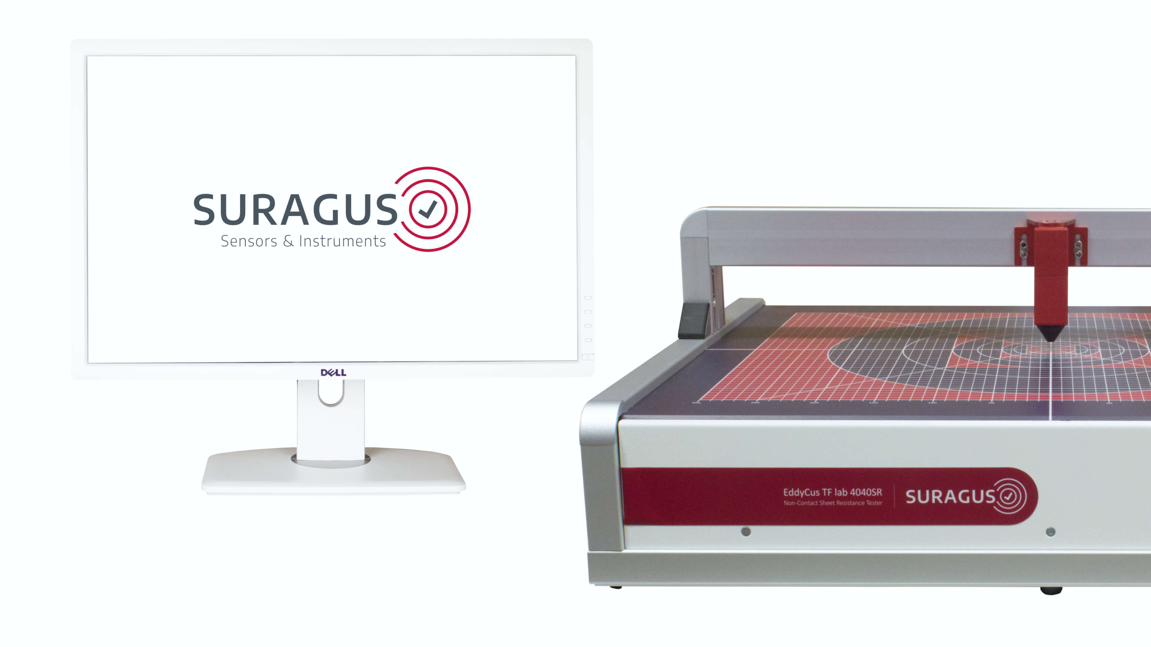
The EddyCus® TF lab 4040SR is a non-contact single point sheet resistance measurement system. The device contains an eddy current sensor set that induces weak currents into conductive films and material. The induced currents in the specimen generate an electromagnetic field that correlates with the sheet resistance of the measure object. The technology is independent from surface characteristics or morphology. Furthermore, it does not require any sort of sufficient specimen contact or preparation such as known from 2- or 4-point probe testing (2PP, 4PP) or hall effect or Van-der-Pauw measurements. It neither requires the setup of test structures nor it is affected by surface roughness or non-conductive encapsulations or passivation layers. Additionally, the measurement does not physically affect the tested thin-film. Eddy current Instruments have a long-life time since there is mechanical wearing. Its independence from contact qualities and its high speed allows enables high repeatability and the accuracies that are beneficial for systematic quality assurance of various thin-films in R&D and testing laboratories. The EddyCus tools can be driven by SURAGUS software with various data recording and export functions or by customer software driven by SURAGUS software development kits.
| Measurement technology | Non-contact eddy current sensor |
| Substrates | Foils, glass, wafer, etc. |
| Substrate area | 29.5“ x 25.6“ / 750 mm x 650 mm (for 400 mm x 400 mm samples) |
| Max. sample thickness/ sensor gap | 3 / 5 / 10 / 25 mm (defined by the thickest sample) |
| Thickness measurement range of metal films (e.g. copper) | 2 nm – 2 mm (in accordance with sheet resistance (cf. our calculator)) |
| Device dimensions (w/h/d) | 30“ x 12“ x 26“ / 760 mm x 310 mm x 660 mm |
| Weight | 20 kg |
| Further available features | Sheet resistance measurement, Metal thickness tester, Anisotropy sensor , Optical transmittance, reflectance, haze |
| VLSR | LSR | MSR | HSR | VHSR | |
|---|---|---|---|---|---|
| 6 decades are measurable by one sensor, but with slightly affected accuracy | |||||
| Range [Ohm/sq] | 0.0001 – 0.1 | 0.1 – 10 | 0.1 – 100 | 10 – 2000 | 1,000 – 200,000 |
| Accuracy / Bias | ± 1% | ± 1 – 3% | ± 3 – 5% | ||
| Repeatability (2σ) | < 0.3% | < 0.5% | < 0.3% | ||
| VLSR – Very Low Sheet Resistance , LSR – Low Sheet Resistance , MSR – Medium Sheet Resistance , HSR – High Sheet Resistance , VHSR – Very High Sheet Resistance | |||||
You are welcome to contact our team for
 |
 |
 |
 |
 |
 |
 |
 |
The EddyCus® TF lab 4040MT allows the non-contact metal thicknesses measurement of transparent and non-transparent layers. The measurement is achieved using a non-contact eddy current sensor. It demines the metal thickness of materials with known or (rather) constant conductivity in real-time. This non-contact testing technology enables a precise measurement in a wide thickness range starting at a few nanometer thickness reaching up to the characterization of thick metal sheets and plates. The technology is also able to characterize metal layers that are covered by non-conducive materials. SURAGUS offers material specific setups for very thin layers and also very thick metals and common alloys. The measurement method is extremely robust and excels with a high repeatability and high accuracy. Additionally, it does not require any optical transparency nor to apply a physical contact. Therefore, it is used for a wide range of application for quick tests or systematic quality assurance.
| Measurement technology | Non-contact eddy current sensor |
| Substrates | Foil, glass, wafer, etc. |
| Substrate area | 29.5“ x 25.6“ / 750 mm x 650 mm (for 400 mm x 400 mm samples) |
| Max. sample thickness/ sensor gap | 3 / 5 / 10 / 25 mm (defined by the thickest sample) |
| Metal thickness range Accuracies depend on the selected setup and the type / conductivity of the metal (e.g. copper, aluminum, silver) |
Low 1 – 10 nm; 2 – 5 % accuracy Standard 10 – 1,000 nm; 1 – 3 % accuracy High 1 – 100 µm; 0.5 – 3 % accuracy |
| Metal thickness calibration | Direct thickness calibration / sheet resistance conversion |
| Device dimensions (w/h/d) | 30“ x 12“ x 26“ / 760 mm x 310 mm x 660 mm |
| Weight | 20 kg |
| Further available features / other tool configurations | Sheet resistance measurement / conductivity / resistivity / emissitivity / permeability (beta) / electrical anisotropy / optical transmittance / optical reflectance / haze |
You are welcome to contact our team for
|
|
|
|
|
|
|
|
|
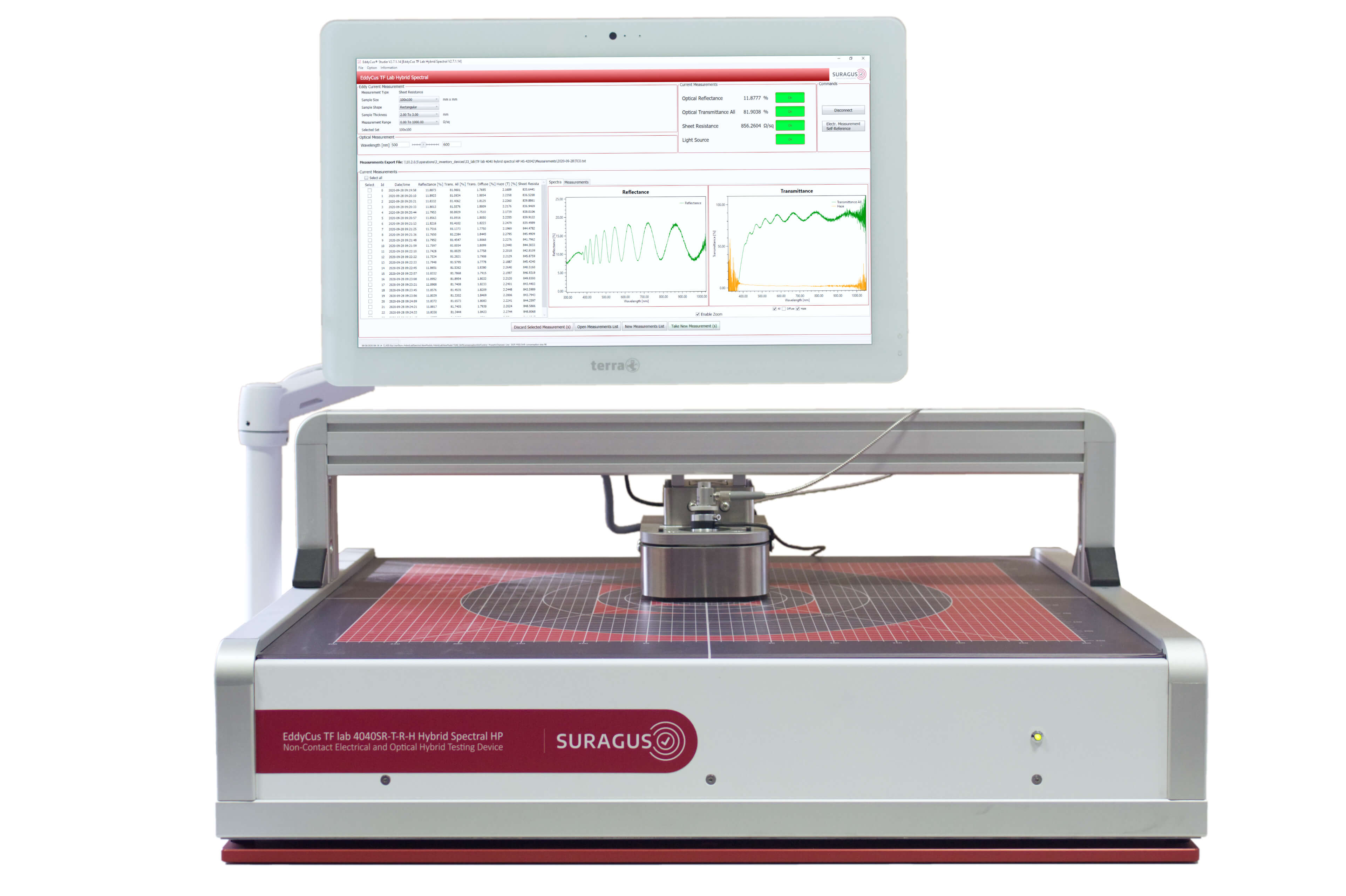
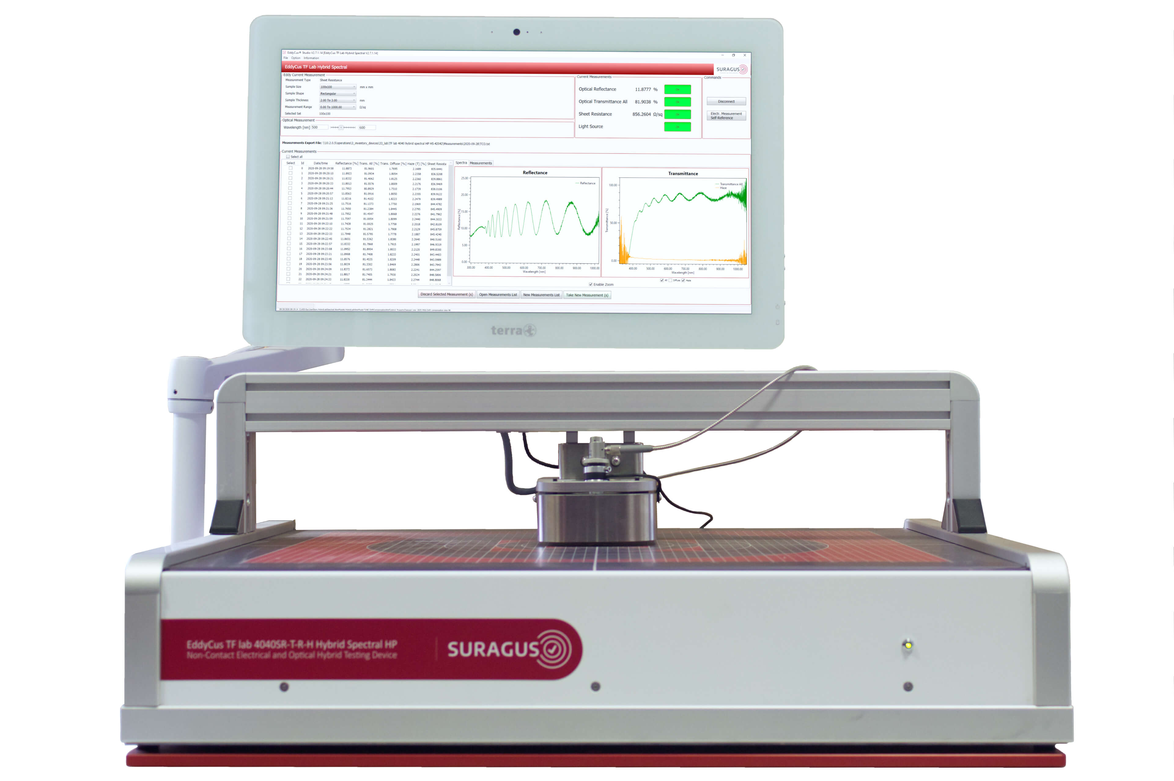
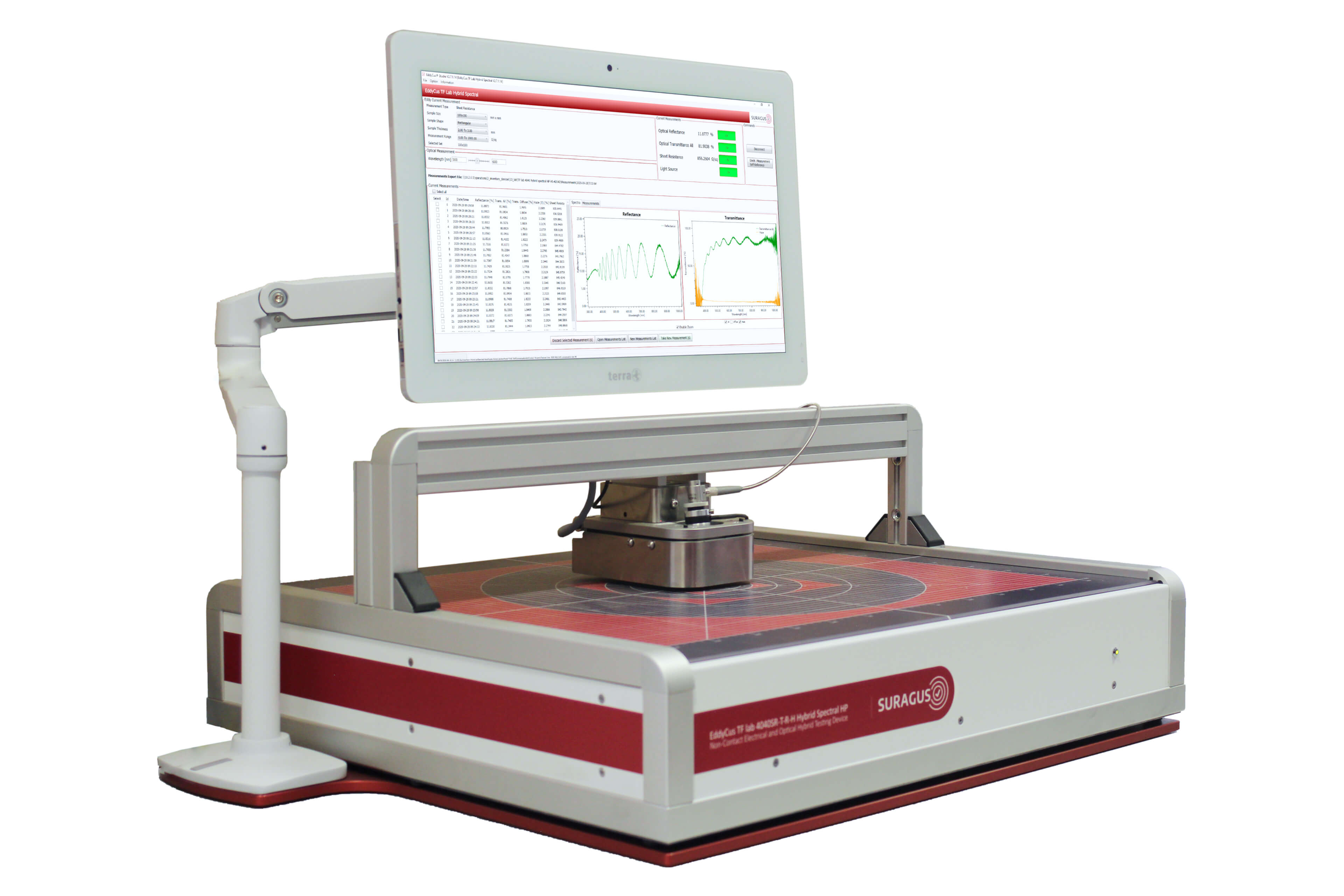
The EddyCus® TF lab 4040HS allows the simultaneous measurement of:
It is a compact hybrid benchtop device that is dedicated to the needs of developers and manufacturer of transparent conductive materials (TCM). It precisely determines in non-contact the two main functions of transparent conductive materials: its optical transparency/ density and its sheet resistance. It supports the systematic characterization and quality assurance for deposition, doping and annealing processes in a variety of materials for research and development as well as for manufacturing companies.
| Measurement technology | Non-contact eddy current sensor and optical sensor |
| Substrates | Foils, glass, wafer, etc. |
| Substrate area | 29.5“ x 26.5“ / 750 mm x 650 mm (for 400 mm x 400 mm samples) |
| Max. sample thickness / sensor gap | 1 / 2 / 5 / 10 mm (defined by the thickes sample) |
| Sheet resistance range | Standard 0.01 – 1,000 Ohm/sq; 1 to 5 % accuracy |
| Thickness measurement of thin films (e.g. Copper) | 2 nm – 2 mm (in accordance with sheet resistance) |
| Spectral resolution* | 0.27 nm |
| Spectral optical transmittance, reflectance range | 0 – 100 % , resolution of 0.1 % |
| Spectral range* | 400 – 1,100 nm or 220 – 2,000 nm |
| Integration time | 1 s or 50 ms – 10 minutes |
| Device dimensions (w/h/d) / weight | 30“ x 12“ x 26“ / 760 mm x 310 mm x 660 mm / 30 kg |
| Further available features | Spectral haze measurement in transmission |
You are welcome to contact our team for
 |
 |
 |
 |
 |
 |
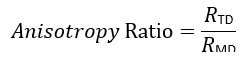
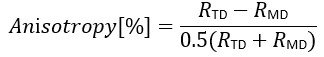
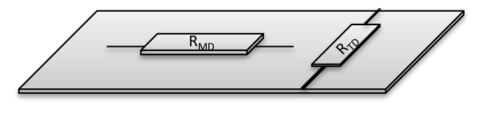
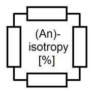
The EddyCus® TF lab 4040A (Anisotropy) is dedicated to the measurement of the electrical anisotropy and the sheet resistances in certain directions. It is relevant especially for functional thin-film that need to be conductive mainly in a certain direction, while achieving highest optical transparencies. This novel device is equipped with integrated sheet resistance anisotropy sensors. The sensors induce currents, which are directed into machine and traverse direction. The results of these directed sheet resistances are used to precisely reflect the electrical anisotropy. This non-contact testing method provides results in real-time and prevents time consuming destructive testing. It is used for fast tests and systematic quality assurance in various industries.
| Measurement technology | Non-contact eddy current sensor with directed current induction |
| Substrates | Foils, glass, wafer, etc. |
| Substrate area | 29.5” x 25.6” / 750 mm x 650 mm (for 400 mm x 400 mm samples) |
| Max. sample thickness / sensor gap | 3 / 5 / 10 / 25 mm (defined by the thickest sample) |
| Sheet resistance range | 0.01 – 1,000 Ohm/sq; 1 to 5 % accuracy |
| Anisotropy range (TD/MD) | 0.33 – 3 (larger upon request) |
| Device dimensions (w/h/d) | 30” x 12” x 26” / 760 mm x 310 mm x 660 mm |
| Weight | 20 kg |
| Further available features | Metal thickness, optical transmittance and reflectance, sheet resistance, emissivity, resistivity and anisotropy measurement |
You are welcome to contact our team for
 |
 |
 |
 |
The EddyCus® TF map 4040HF is a high frequency eddy current single point measurement device designed for material and thin-film characterization. The device is sensitive to characteristics that correlate with electric, dielectric and magnetic properties. Typical applications include the assessment of material composition, the measurement of residual moisture, wet coating thickness or permittivity, and the determination of the content level of conductive (e.g. C, Pt) or magnetic (e.g. Co) materials. SURAGUS also supports complex impedance analysis to derive information on electrical, dielectric or magnetic properties from hybrid materials with a single measurement. The exact capabilities regarding specific measurement tasks can be provided from a consultation with the SURAGUS team.
| Measurement technology | Non-contact high frequency eddy current sensor |
| Substrates | Foils, glass, various containers |
| Substrate area | 750 mm x 650 mm / 29.5“ x 25.6“ (for 400 mm x 400 mm samples) |
| Max. sample thickness/ sensor gap | Transmission setup: 3 – 50 mm (defined by the thickest sample) Reflection setups: infinite (only surface area is analyzed) |
|
Measurement types |
Wet thickness (µm) / weight (g/m²) / drying status (%) / conductivity (MS/m) / resistivity (mOhm cm) / permeability (H/m) Beta / permittivity (F/m) Beta |
| Measurement range / accuracy | Depends on the measurement task, the material composition and the test object volume. Please consult the SURAGUS team |
| Device dimensions (w/h/d) | 30“ x 12“ x 26“ / 760 mm x 310 mm x 660 mm |
| Weight | 20 kg |
| Further available measurements | Sheet resistance, metal thickness, anisotropy, optical transmittance, reflectance, haze |
You are welcome to contact our team for
|
|
|
 |
|
|
|
For product requests contact us by using the