Quality Assurance using Eddy Current Testing
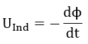
The eddy current testing method utilizes local conductivity variations for the characterization of quality characteristics such as thickness, sheet resistance, material homogeneity or other physical changes in the sample of investigation. The complex eddy current signal contains various information about the test material, which can be separated in many cases with simple or complex algorithms. The applied powerful eddy current electronics offers a wide frequency range from 10 kHz to 100 MHz that is utilized to achieve different sensitivities and penetration depth depending on the application. All SURAGUS products are offered with an user-friendly software for fast real-time evaluation.
Process
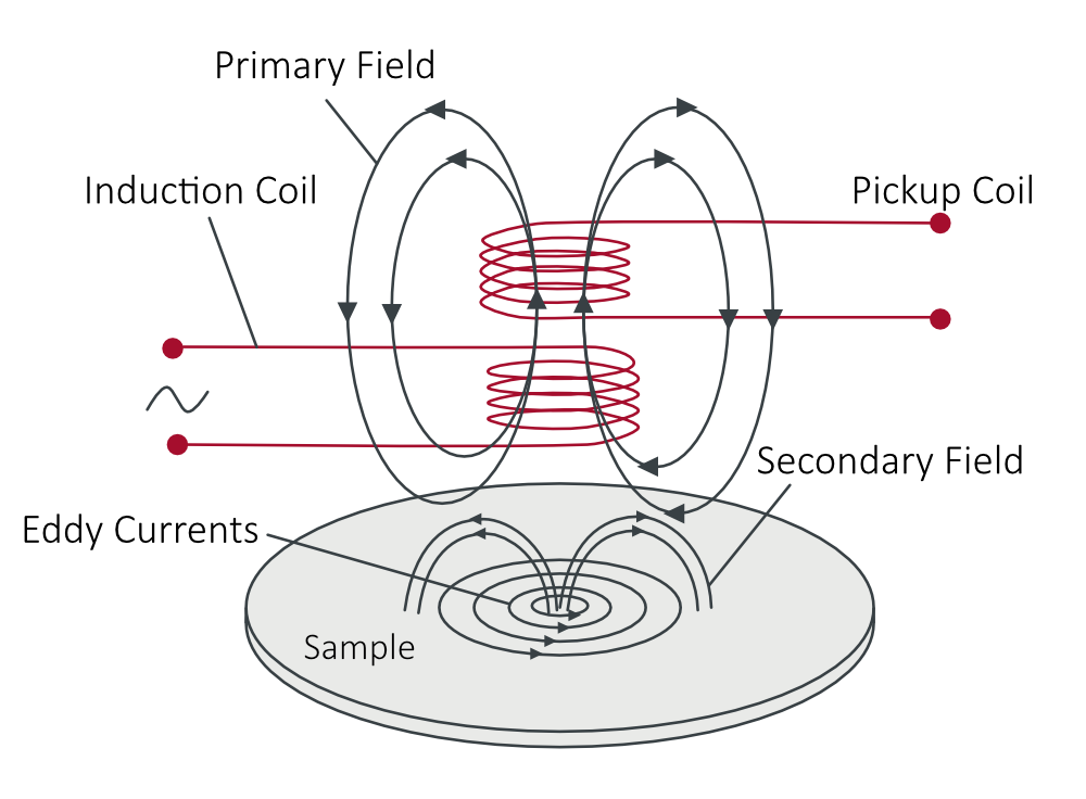
The eddy current testing method is a nondestructive evaluation method. It is widely used for crack detection as cracks cause very large local conductivity changes. However, there are many other applications in which highly sensitive and spatially resolved conductivity analysis can help to solve various inspection tasks. The basic principle is shown below.
Non-contact testing solution for different applications:
- Sheet resistance
- Resistivity
- Metal layer thickness
- Electrical anisotropy
- Distance (to conductive materials) / paint thickness
- Carbon fiber testing
- Composition monitoring
Characteristics
- Contactless and non-destructive
- Extremely fast / high sample rates (k samples / second)
- Good automation abilities
- High sensitivity
Eddy Current Density
Since the sensitivity of eddy current inspection depends on the eddy current density at the defect location, it is important to consider the strength of the induced eddy currents at the defect location. Typically, a setup / frequency / sensor is selected which places the expected defect within a one standard penetration depth. This assures that the strength of the eddy currents would be sufficient to produce a flaw indication.
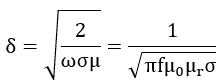
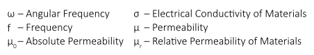
Penetration depth depends on to the permeability, conductivity of the material as well as the frequency.
Standard Penetration Depth
The standard penetration depth is a term that is relevant to select a good testing setup for the characterization bulk materials. The depth that eddy currents penetrate into a material is affected by the frequency of the alternating current, the electrical conductivity and magnetic permeability of the sample. The depth of penetration decreases with increasing frequency and increasing conductivity and magnetic permeability. The depth at which eddy current density has decreased to 1/e, or about 37% of the surface density, is called the standard depth of penetration (d or 1d) and is used as criteria of ideal measurement for the investigation of bulk materials. At three standard depth of penetration (3d), the eddy current density is down to only 5% of the surface density. So, defects or variation in deeper depth than this do not add recognizable to the measurement effect and therefore those are hardly detectable. Thus, a setup that achieves a standard penetration depth suitable (1d) to the depth of the characteristics of interest enables the best testing result. SURAGUS offers a wide range of sensors with different frequency ranges for optimum testing of materials with different properties.
Eddy Current Impedance
- X is the real part
- Y is the imaginary part
- Z is the magnitude
- Φ is the phase
- Rotated phase plot
At a given frequency and position the eddy current value is at P0. When bringing a sample into the field or moving it to a different location the complex value shifts towards P1.
Capacitive and resistive effects can be separated by interpreting the data. For example by projecting on x- or y-axis.
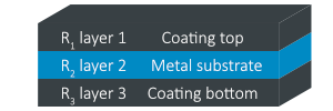
Measurement of Encapsulated Layers
One of the biggest advantages of the eddy current method compared to the four-point method is the possibility to measure hidden layers. A hidden layer is a layer that lies beneath another and is therefore not accessible from the outside. This is possible due to the characteristic of the eddy current method, which does not require direct contact with the layer under investigation. It works very effectively even at a distance of several millimeters from the layer or material under investigation.
For example, a non-conductive substrate might have an electrically conductive layer deposited underneath an insulating layer. In such cases, the eddy current method can characterize the conductive layer. It is even possible to separate different conductive layers from each other as long as their conductivities differ significantly. For a precise assessment of whether your particular application can be measured, please contact our team.
Contact Us For More Information
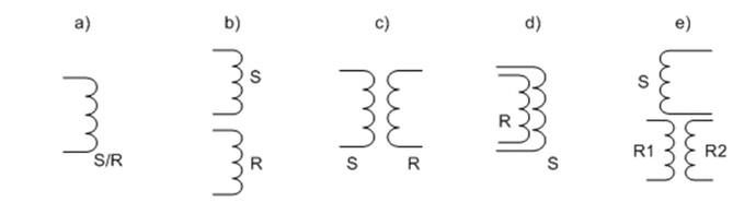
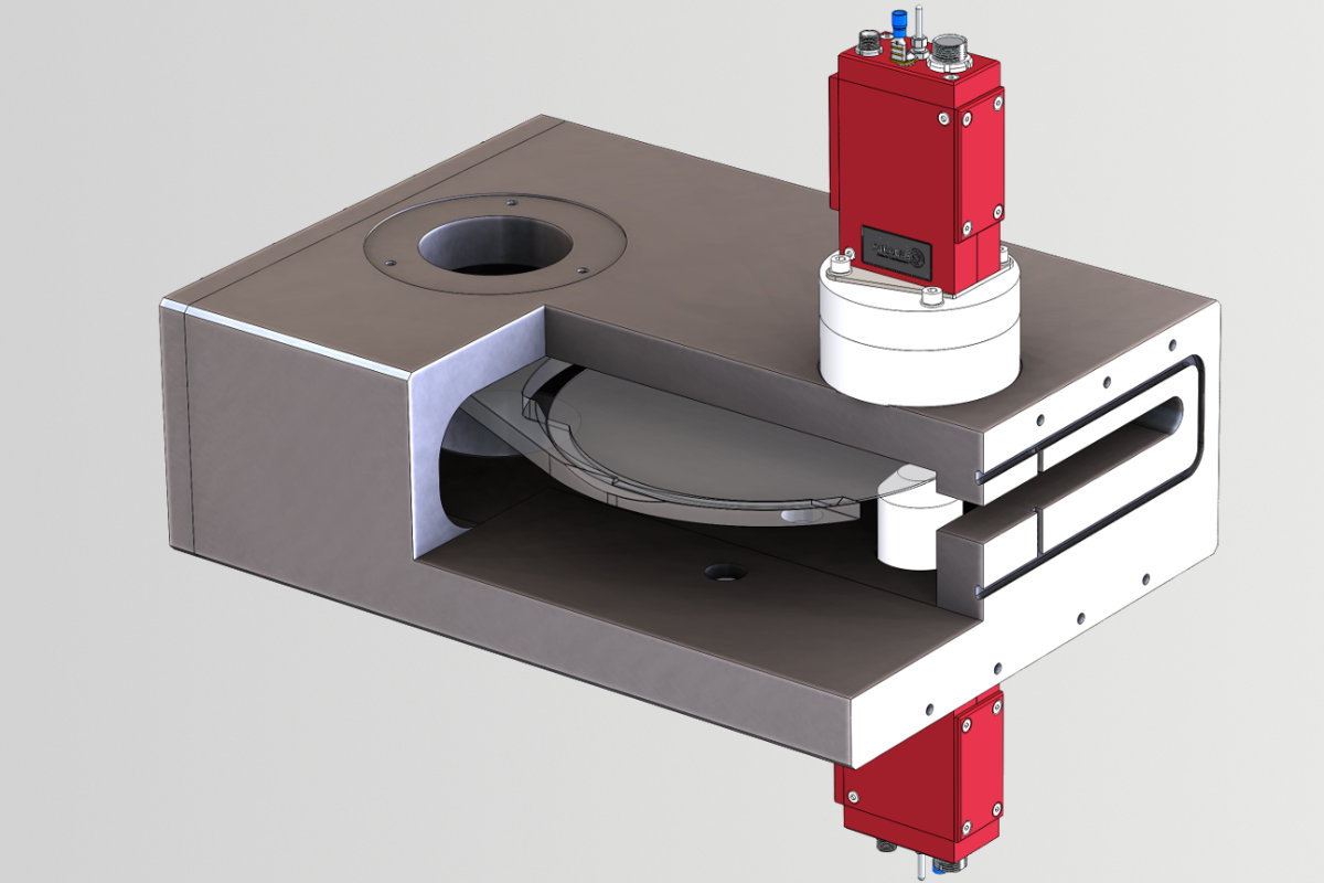
Eddy Current Sensors
Types of Eddy Current Sensors
- Sender: inductive coils
- Receiver: inductive coils, hall sensors, fluxgate sensors, GMR, SQUIDs
Types of Eddy Current Testing
- Single frequency
- Multi-frequency
- Spectral
- Impulse eddy current
- Etc.
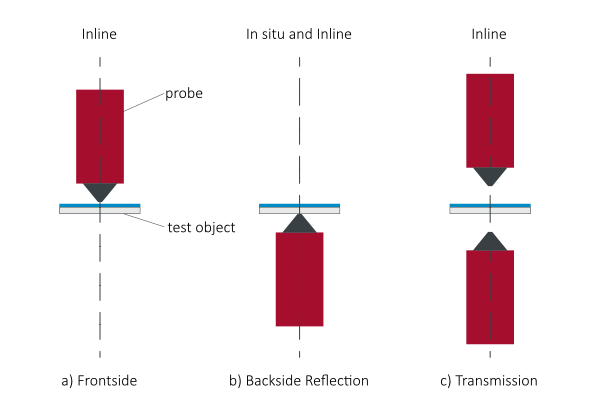
Setup of Layer Characterization
- Frontside reflection mode
- Backside reflection mode
- Transmission mode
Eddy current measurement setups include single-sided and double-sided setups. Both are widely used but there are advantages and disadvantages to each approach.
Double side transmission mode sensors and tools operate in large distances to the wafer and excel with high tolerance to vertical wafer surface positions. This means the same set can be used for immediate measurement of thin and thick wafers without requiring time consuming set up changes. With large sensor elements gaps up to 100 mm makes double sided transmission ideal for robot handling and the integration into process tools without requiring additional tool space or processing time.
Reflection mode (single side resp. frontside or backside) tools are best for small spot sizes down to 1 mm. The tradeoff is that precise distance control and comes with limitations in sensitivity. This enables penetration depth modification, which allows focusing on resistivity measurements to the surface regions of SiC, GaAs and Si materials on ingot and boule level.
Benefits of Wide and High Frequency Testing
Relevance of Frequency
- The frequency determines the signal strength
- Low sheet resistance materials require lower frequencies
- High sheet resistance materials require higher frequencies
Flexibility in the frequency range supports wide measurement range setups enabling the measurement over 6 decades with the same setup.
Eddy Current Imaging vs 4 PP Mappings – Measurement Points Are Key
Eddy current imaging offers significant advantages over traditional 4-point probe (4PP) mapping. While 4PP systems typically collect data at a limited number of discrete points, eddy current imaging captures tens of thousands of measurement points per wafer, enabling a far more detailed and spatially resolved analysis.
SURAGUS imaging systems support standard scan pitches of 2.5 mm, with flexible options ranging from 10 mm down to 0.1 mm, depending on the required resolution. For example, scanning a 200 mm wafer at a 2.5 mm pitch yields over 5,000 individual data points, while a 1 mm pitch results in more than 30,000 real measurements within 1 minute.
The higher point density provides richer datasets, supporting more accurate process control, defect detection, and uniformity analysis—essential for optimizing yield and maintaining quality in advanced semiconductor manufacturing.
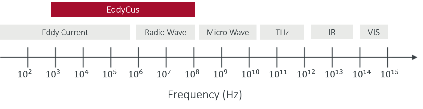
Mapping Quality Comparison – EC vs 4PP
In the image shown, the same wafer is measured using two different methods: SURAGUS eddy current imaging (left) and a 49-point 4-point probe (4PP) mapping system (right). Two key differences are immediately apparent:
- Wafer Coverage: The eddy current system captures measurements across the entire wafer, including the edge region. In contrast, 4PP systems are restricted to the 49 point pattern that exclude the wafer edge, resulting in missing data near the periphery. Some tools attempt to extrapolate edge values based on the outermost measurement ring, but this does not provide true measurement data.
- Spatial Resolution and Feature Detection: The eddy current image reveals a small structure in the wafer center that is completely absent in the 4PP map. This is due to the limited number and spacing of measurement points in 4PP systems. When no probe lands directly on a localized feature, and the spacing between points is too large, interpolation fails to capture small or localized variations. Eddy current imaging, with its dense and continuous data acquisition, provides superior spatial resolution, enabling the detection of subtle or localized conductivity variations that are otherwise missed.
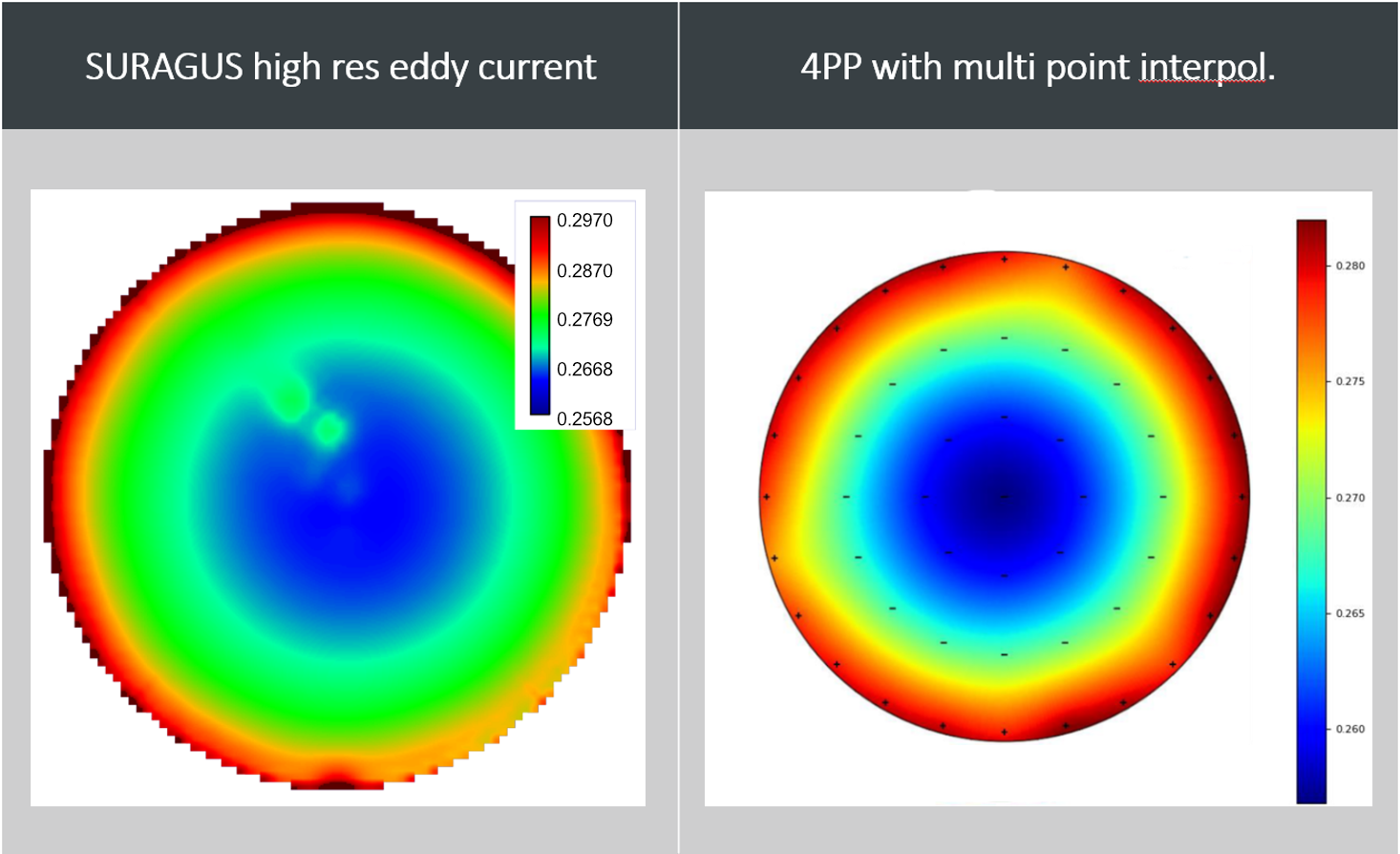
Measurements Close To The Edge
The scan resolution of eddy current imaging is high enough to accurately resolve the steep sheet resistance gradient at the facet transition. Despite the facet being located directly at the physical edge of the wafer, the measurement clearly captures the sharp drop in sheet resistance, followed by a precise rise back to the nominal value on the inner wafer surface.
This demonstrates the high spatial resolution and sensitivity of the eddy current method – even in challenging edge regions where conventional systems struggle or cannot measure at all. The technology delivers fast, non-contact, and highly accurate measurements, making it well-suited for advanced process monitoring and R&D applications.
Testing Directly On Production Wafer
Due To Non-contact Eddy Current Technology
Traditionally, 4-point probe (4PP) systems have required the use of dedicated test wafers, as the measurement method involves direct physical contact with the wafer surface, which can introduce contamination, surface damage, or stress. As a result, many production environments had to adapt their processes by including test wafers in each batch—adding time, cost, and complexity to routine monitoring.
However, with the introduction of eddy current measurement technology, these limitations are no longer a concern. This non-contact technique enables direct measurements on production wafers without any risk of mechanical impact or contamination. Eddy current sensors operate through electromagnetic induction, allowing for fast, accurate, and repeatable measurements of sheet resistance, metal layer thickness, resistivity and uniformity across the entire wafer surface—including the edges and sensitive thin films.
By enabling inline or at-line characterization on actual product wafers, eddy current measurement eliminates the need for surrogate test wafers and provides more relevant process data, enhancing both quality control and yield management. Manufacturers can now gain real-time insight into their processes while reducing material waste and improving overall efficiency.
Superior Properties of Non-contact Testing
| 4-Point-Probe Testing | Non-contact Eddy Current Testing |
| Contact quality influences measurement | Non-contact & real-time, no wearing |
| Single point and mapping solutions |
Single point measurement High resolution mapping Inline measurement encapsulated films |
| Possible damage to sensitive layers | No harm or artifacts to sensitive films |
| Wearing of probe with time | High accuracy without influence of contact resistance |
| No measurement of encapsulated films | Encapsulated films & multilayer systems |