For product requests contact us by using the
- Contact formular,
- Email (sales@suragus.com) or
- Phone (+49 351 32 111 520).
Different high effiency wafer based cell technologies are available in high volume manufacturing. Manufacturing costs are crucial for cells and modules. For achieving highest efficiency at lowest manfacturing cost, the following deposition processes have to be monitored:
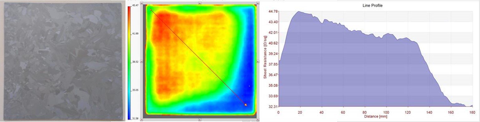
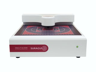
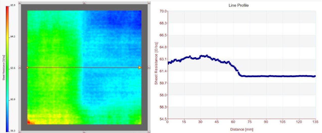
Wafer incoming inspection for poly or mono Si wafer is dedicated to sheet resistance characterization by means of high frequency eddy current technology. Measurement tasks could be realized by individual sheet resitastance characteriztation or combined with thickness measurement.
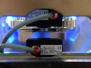
Passivation of wafer for minimizing recombination effects can be monitored by inductive methodes such as hogh frequency eddy current technology.
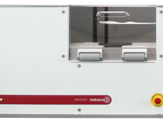
For incoming inspection and characterization of deposition processes in crystalline photovoltaics SURAGUS refers to the following products:
For product requests contact us by using the