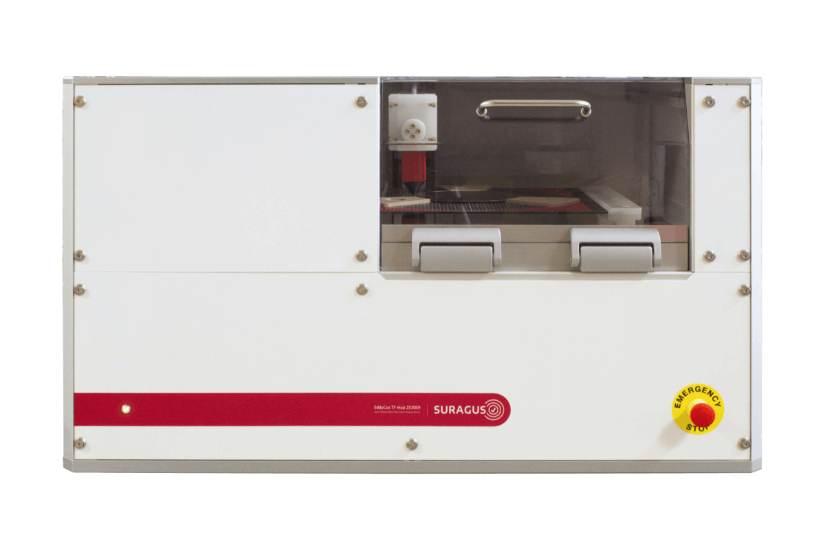
Non-contact Sheet Resistance and
Metal Layer Thickness Mapping Device
Improve thin-film and substrate quality with fast, precise, non-contact mapping. The device accurately measures sheet resistance and correlating parameters in wafers, foils, glass, and metallized layers.
- Non-contact
- Fast and precise measurement
- High resolution mapping of conductive thin films
- Imaging of substrates up to 300 x 300 mm (12 x 12 inches)
- Characterization even of hidden and encapsulated conductive layers
- Various software-integrated analysis functions (e.g. sheet resistance distribution, line scans, single point analysis)
- Measurement data saving and export functions
- Defect detection and coating analysis
Introduction
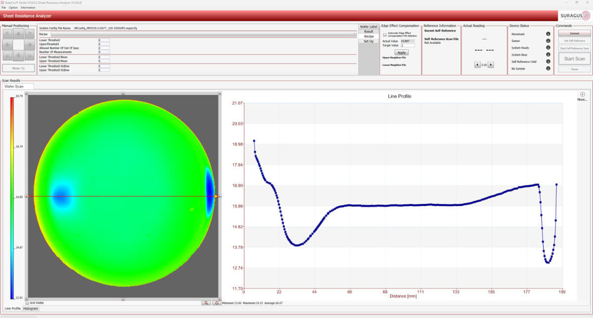
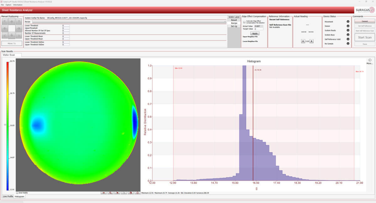
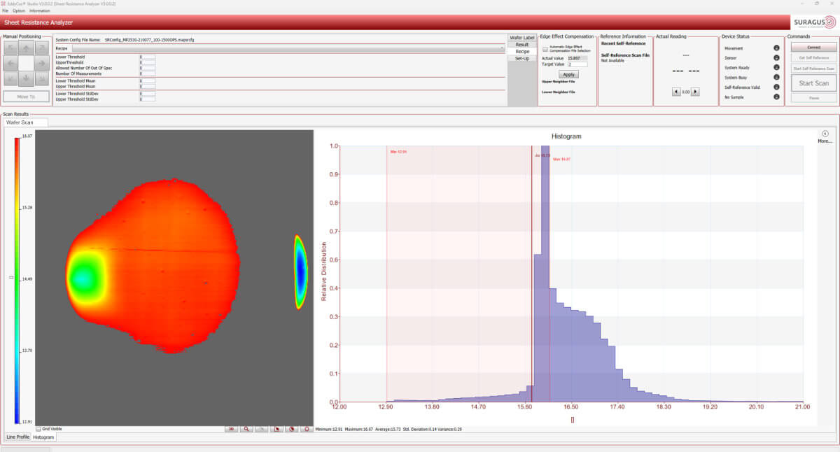
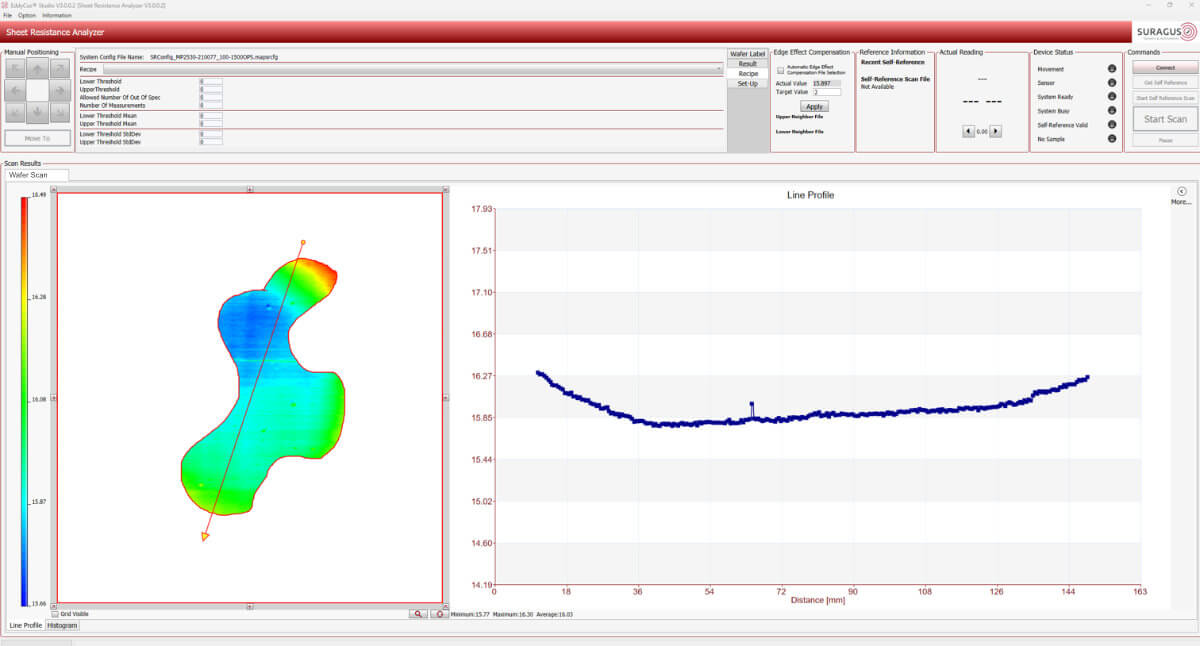
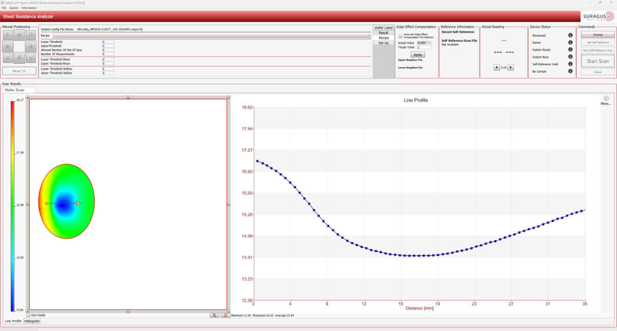
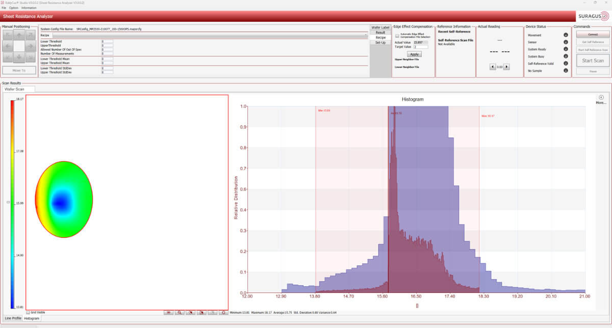
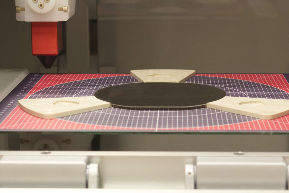
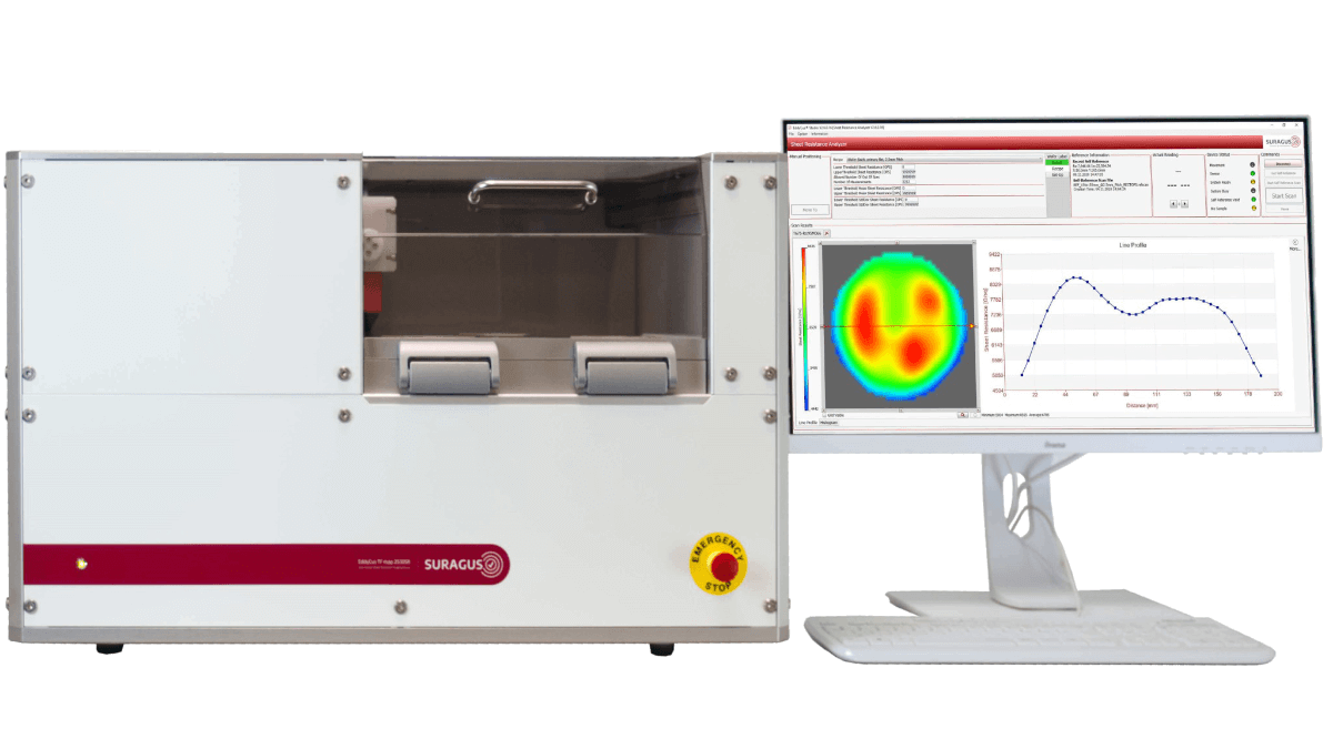
The EddyCus® map 2530 TM series automatically measures the sheet resistance of large samples up to 300 × 300 mm² (12 × 12 inches) in non-contact mode. After manual placement of the sample, the system performs a fully automated scan and generates a high-resolution sheet resistance map across the entire surface.
The tool uses a stationary eddy current sensor, while the sample stage moves to enable scanning. This design allows for measurements on the fly, with no physical contact required, eliminating errors due to contact resistance. Depending on the selected settings, users can prioritize fast measurement times (under 1 minute) or high spatial resolution (up to 90,000 measurement points per scan).
The non-contact measurement ensures high accuracy and repeatability, independent of surface condition or contact quality. The dense measurement grid enables reliable detection of material variations, inhomogeneities, and defects. The included software offers a wide range of advanced analysis tools, supporting systematic quality control of thin films in both manufacturing and research environments.
The device is typically used for:
- Technology: non-contact eddy current
- Imaging by multipoint mapping
- Sampling area: 300 x 300 mm
- Recommended sample sizes: 1 inch to 12 inch or 25 to 300 mm

Sensor Capabilities
- Sheet Resistance [0.00005 – 300,000 Ohm/sq]
- Metal Layer Thickness [1 nm – 100 µm]
- Resistivity [depending on the sheet resistance]
- Electrical Anisotropy [0.33 – 3]
Supported Sample Thickness
2 – 4 mm fixed sensor (customized upon request)
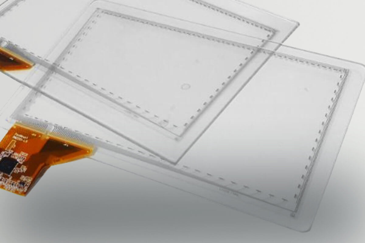
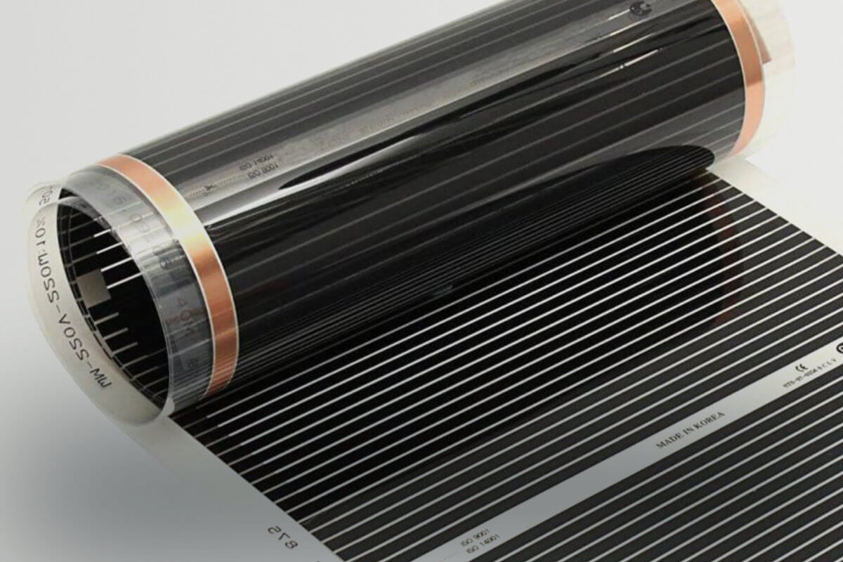
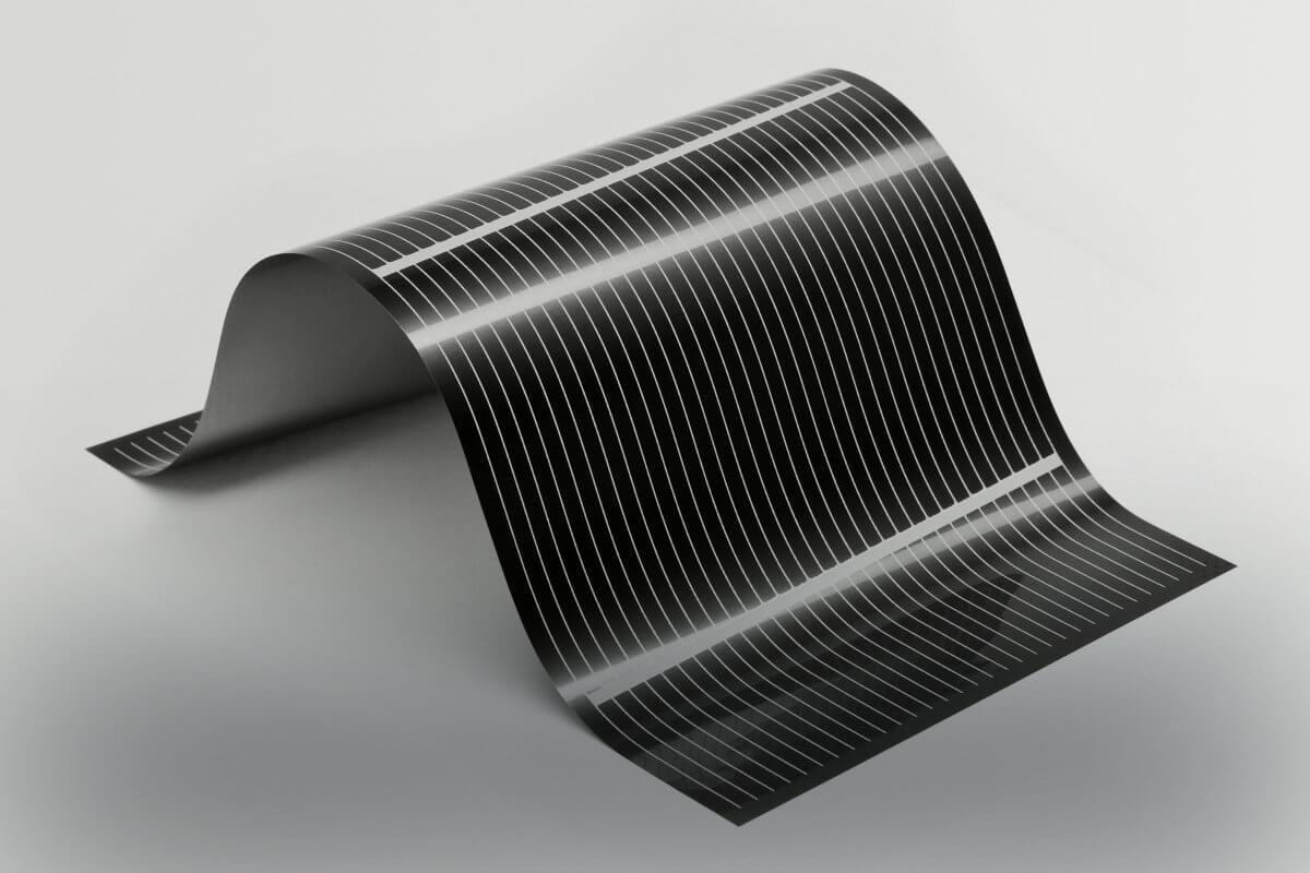
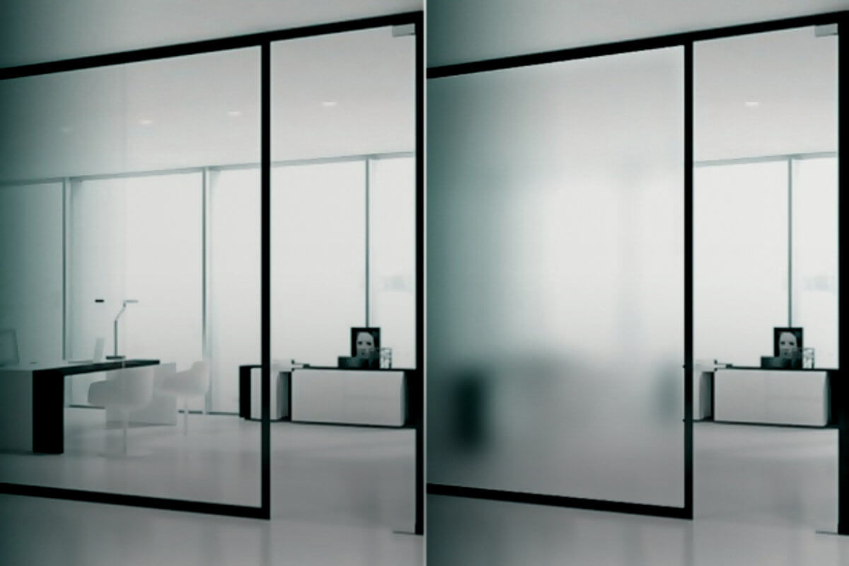
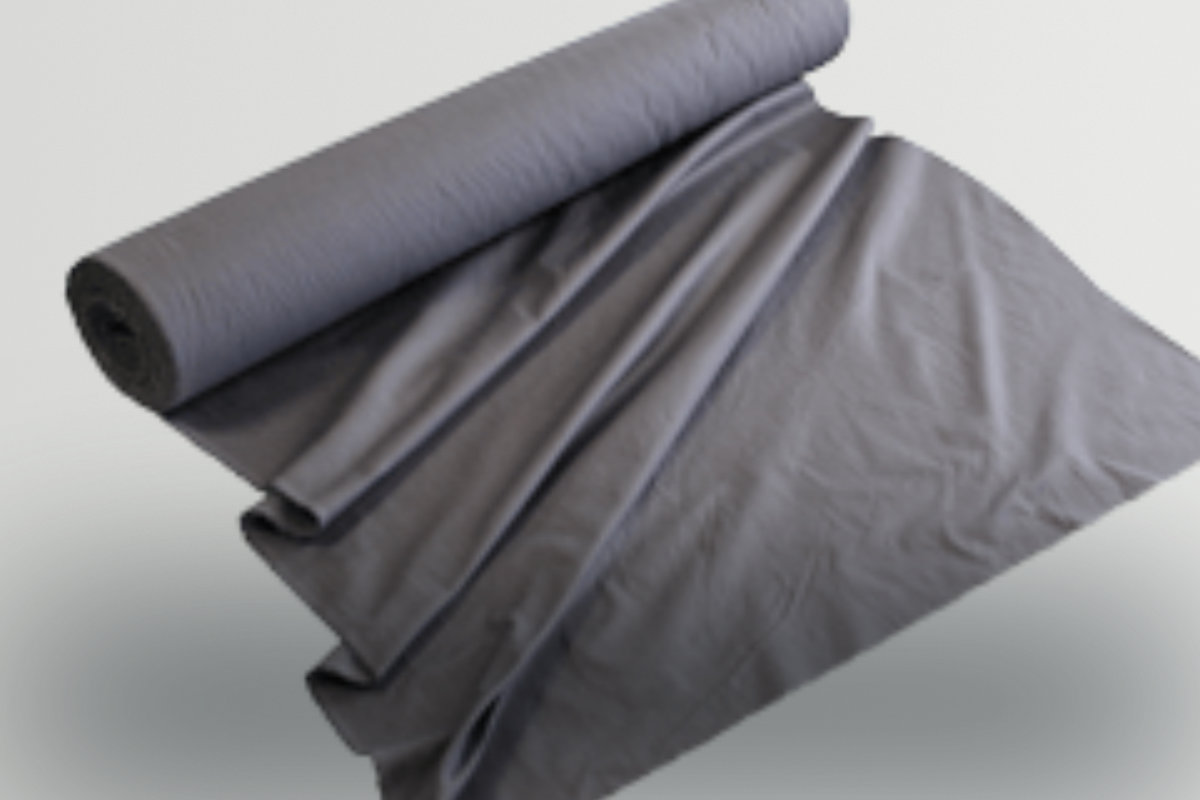
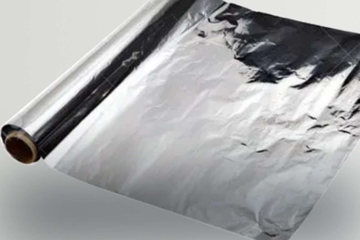
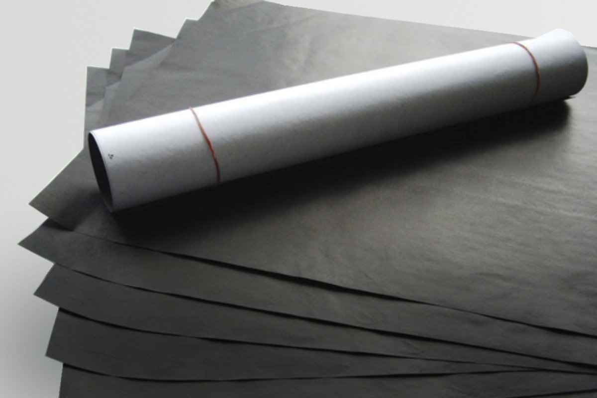
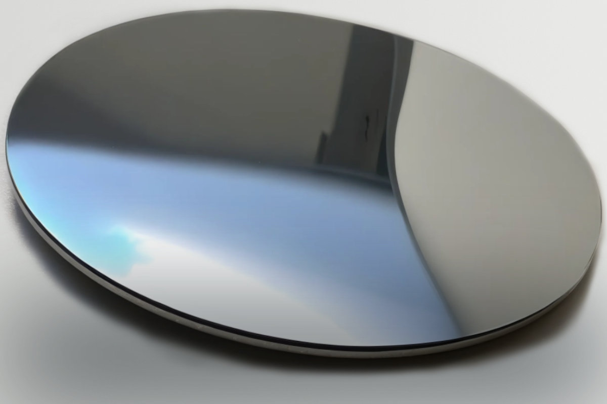
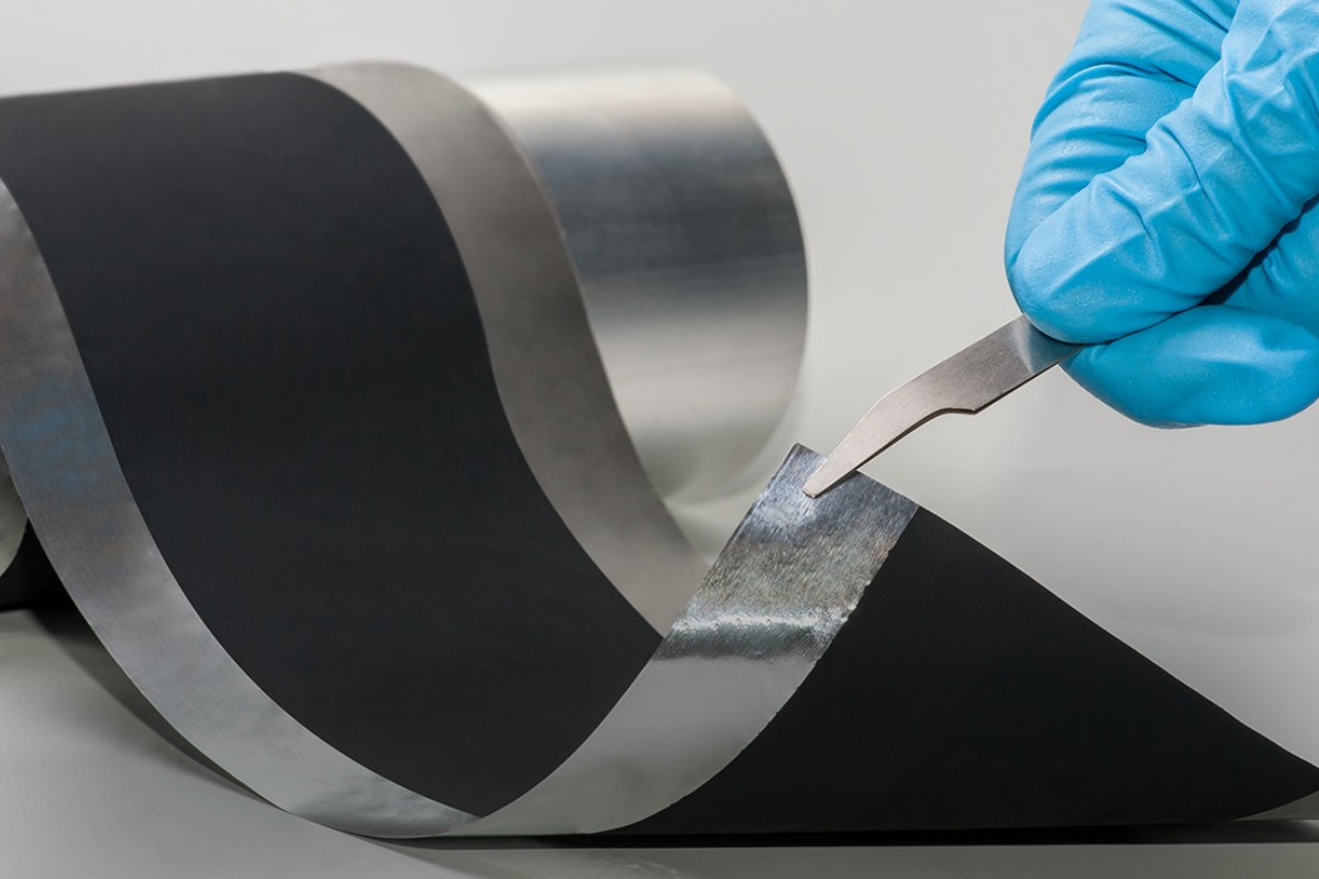
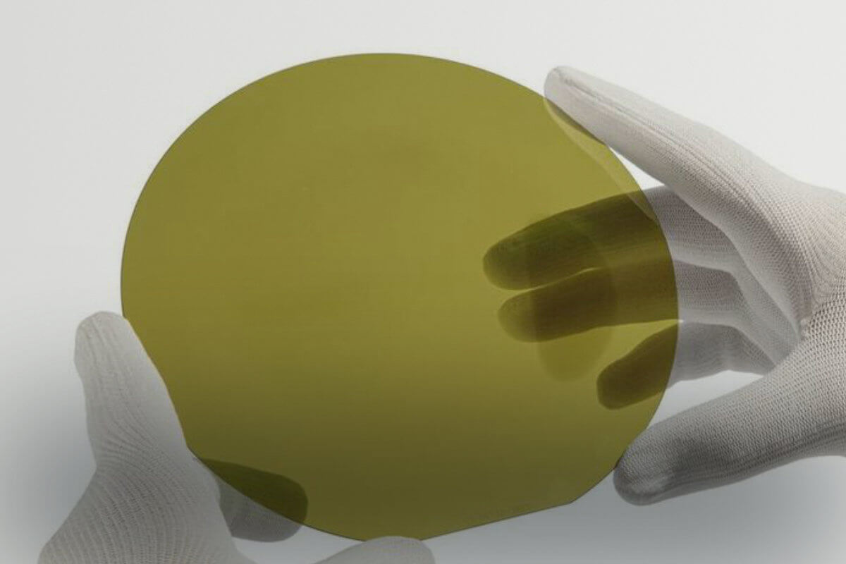
Supported Substrates
Foils, glass, wafer, solar wafer, e. g.
Each sample with a maximum high of 4 mm
Measurement Field
Sample sizes between 25 mm x 25 mm and 300 mm x 300 mm.
With markings for easy positioning.
Removable Wafer Holder
Accurate measurements require precise central positioning.
To facilitate easy centering, we offer removable wafer holders
compatible with various wafer sizes.
Material: PEEK
Customized sizes between 2 inch – 300 mm
Features and Benefits
2 – 12 Inch
6 Decades
Various Analyzing Options
Fast Results
High Resolution Mappings
Easy to Use
3D Viewer
One Device, Multiple Measurement Parameters
The EddyCus® map 2530 TM is capable of measuring multiple parameters. Sheet resistance correlates with metal layer thickness, emissivity, resistivity and conductivity. As long as the material properties are well known, all of these parameters can be measured with high precision. In addition, the device is able to determine the anisotropy of the sheet resistance.
- Sheet resistance
- Metal layer thickness
- Electrical Anisotropy
- Emissivity
- Resistivity
- Conductivity
Software and Device Control
- Very user-friendly software
- Realtime mapping measurement
- Easy-to-use statistical analysis options
- Pre-defined measurement and product recipes (sizes, pitches, thresholds)
- Line scan, histogram and area analysis
- Black and colored image coding
- Csv & pdf export
- PC summary and export
- 3 user level
- Material database for parameter
- conversion
- Edge effect compensation
- Storage and import of data
- Export of data sets (e.g. to EddyEva, MS Excel, Origin)
Video of the EddyCus® map 2530 TM
The video gives you an impression of how to use the map 2530 TM. Which materials can be analysed and how the device works in general.
Areas of Application
Data Table for EddyCus® map 2530 TM
Device Features
| Measurement technology | Non-contact eddy current sensor |
| Substrates | Wafer, glass, foils, etc. |
| Substrate area | 12 inch / 300 mm x 300 mm (larger upon request) |
| Max. sample thickness / sensor gap | 3 / 5 / 10 / 15 mm (defined by the thickest sample) |
| Scanning pitch | 1 / 2.5 / 5 / 10 / 25 mm (other upon request) |
| Measurement points per time (square shaped samples) | 100 measurement points in 0.5 minutes 10,000 measurement points in 3 minutes |
| Scanning time | The scanning time depends on the size of the sample and the pitch. 8 inch / 200 mm x 200 mm in 1 to 10 minutes (1 – 10 mm pitch)12 inch / 300 mm x 300 mm in 2 to 6 minutes (2.5 – 25 mm pitch) |
| Available measurement features | Sheet resistance map Metal layer thickness map Resistivity map Conductivity map Electrical anisotropy map Emissivity map |
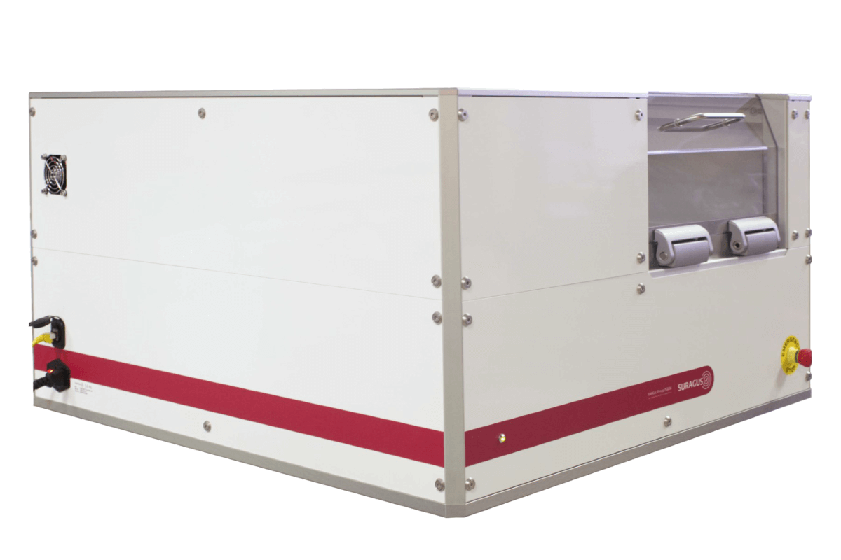
| Device dimensions (w/h/d) | 31.5” x 19.1” x 33.5” / 785 mm x 486 mm x 850 mm |
| Weight | 90 kg |
Measurement Capabilities
| Sheet resistance measurement | |
|---|---|
|
Sheet resistance measurement range (Four sensor setups available) |
Very low: 0.05 – 300 mOhm/sq; 1 – 3 % accuracy Low: 0.001 – 100 Ohm/sq; 1 – 3 % accuracy Wide range: 0.001 – 20,000 Ohm/sq; 1 – 5 % accuracy High: 100 – 300,000 Ohm/sq; 1 – 5 % accuracy |
| Thickness measurement range of metal films (e.g. copper) | 2 nm – 2 mm (in accordance with sheet resistance (cf. our calculator)) | Metal layer thickness measurement |
|
Metal thickness range Accuracies depend on the selected setup and the type / conductivity of the metal (e.g. copper, aluminum, silver) |
Low 1 – 10 nm; 2 – 5 % accuracy Standard 10 – 1,000 nm; 1 – 3 % accuracy High 1 – 100 µm; 0.5 – 3 % accuracy |
| Sheet resistance measurement range | 0.1 mOhm/sq – 100,000 Ohm/sq | Resistivity measurement |
| Resistivity measurement range | In accordance to sheet resistance and layer thickness (cf. our calculator)) | Electrical anisotropy measurement |
| Sheet resistance range | 0.01 – 1,000 Ohm/sq; 1 to 5 % accuracy |
| Anisotropy range (TD/MD) | 0.33 – 3 (larger upon request) | Multi parameter measurement |
| Measurement types |
Wet thickness (µm) / weight (g/m²) / drying status (%) Conductivity / resistivity (mOhm cm) / permeability (H/m) Beta Permittivity (F/m) Beta |
| Measurement range / accuracy | Depends on the measurement task, the material composition and the test object volume. Please consult the SURAGUS team |