Wafer Characterization

In seminconductor industry metal or metal oxide layers are applied for achieving electrical, mechanical, chemical, optical and a plethora of other characterisitcs. Properties such as sheet resistance, conductance, permeability or defectoscopy can be characterized by high frequency eddy current. Standard processes are vacuum processes such as evaporation, sputtering or atomic layer deposition (ALD) and wet processes such as plating. More over several different pre- and post-treatment processes are being used.


Testing

  • Sheet resistance
  • Resistivity
  • Thickness
  • Homogeneity
  • Permeability
  • Defectoscopy
  • Facette formation

Applications

  • Imaging & near edge monitoring
  • Wafer process Monitoring
  • Incoming inspection
  • Quality control
  • Deposition process control
  • Pre- and post-treatment process control

Substrates

  • Silicon
  • SiC
  • GaN
  • Sapphire (Al2O3)

Process

  • Wafer level
  • Batch systems
  • Load lock
  • Cluster systems
  • Inline

Environment

  • In-vacuo and ex-vacuo
  • In-situ and ex-situ
  • Inline and offline

Types

  • Power electronics
  • Industry electronics
  • IC
  • MEMS
  • Microelectronics
  • Microprocessor
  • LED
  • Sensors
  • Optics
  • 5G

Further Resouces

  • SEMI MF673 — Test Method for Measuring Resistivity of Semiconductor Wafers or Sheet Resistance of Semiconductor Films with a Noncontact Eddy-Current Gauge
  • SEMI M59 — Terminology for Silicon Technology
  • SEMI MF81 — Test Method for Measuring Radial Resistivity Variation on Silicon Wafers
  • SEMI MF84 — Test Method for Measuring Resistivity of Silicon Wafers with an In-Line Four-Point Probe
  • SEMI MF374 — Test Method for Sheet Resistance of Silicon Epitaxial, Diffused, Polysilicon, and Ion-Implanted Layers Using an In-Line Four-Point Probe with the Single-Configuration Procedure
  • SEMI MF1527 — Guide for Application of Certified Reference Materials and Reference Wafers for Calibration and Control of Instruments for Measuring Resistivity of Silicon

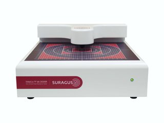
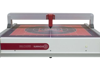
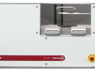
For characterization of wafer processes in semiconductor industry SURAGUS refers to the following product categories:

Contact

For product requests contact us by using the

For a prompt and informative response, please describe your measurement task (material, sample dimensions, expected measurement range) and provide your phone number.

By sending this form, I permit SURAGUS GmbH to process my data for contacting me. For more details see our Imprint & Privacy Policy