For product requests contact us by using the
- Contact formular,
- Email (sales@suragus.com) or
- Phone (+49 351 32 111 520).
With International Technology Roadmap for Semiconductors (ITRS) retiring and International Roadmap for Devices and Systems (IRDS) taking over charge to roadmap the present and future technologies for the next 15 years, there is greater focus to look far more than Beyond CMOS. The introduction of Hetergenous Integration Roadmap (HIR) emphasizes the need to build systems i.e., the integration of independently manufactured components into high-level modules and packages. These assemblies are expected to have significantly improved functionalities and operational performances. With SiP, 3D & 2D interconnects and wafer level packaging (WLP) identified as three major technology areas for heterogenous integration, advanced packaging in semiconductor manufacturing is evolving rapidly by addressing the key drivers:
The 4 leading advanced packaging form factors - fan-out package, SoIC/ Chiplets, 3D TSV/ Interposer, Dual-sided SIPs - are expected to provide high-value solutions for the growing markets:
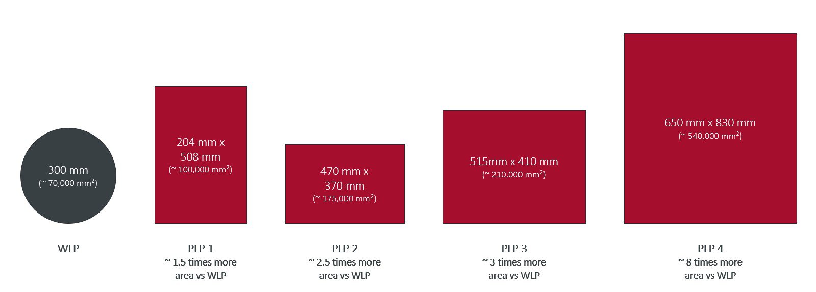
Besides technology developments towards heterogeneous integration, larger substrate formats are also considered. The current manufacturing capabilities on a wafer level goes up to 12"/300 mm. In order to target higher productivity and lower costs, larger form factors are targeted. Although 450 mm is the wafer level roadmap, it could be bypassed to approach panel level packaging (PLP), which might be the next big step. With immense potential to miniaturization and heterogenous integration, both technology approaches offer a lot of opportunities and benefits towards building high-performing systems. The PLP route is expected to follow the established standards in LCD and PCB manufacturing, thereby accelerating development and commercialization goals.
With more area in PLP, more dies are produced, eventually more devices and systems. The large-area metal deposition by PVD and ECD technologies in WLP and PLP are opening new avenues to in-line or offline thin-film characterization, especially by non-contact and non-destructive methods. For the high-throughput requirements, high frequency eddy current technology characterizes sheet resistance, conductivity, thickness and homogeneity of metal layers.
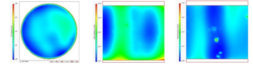
Left: Thickness imaging of Molybdenum on wafer, Middle: Sheet resistance imaging of Titanium on glass for PLP, Right: Sheet resistance imaging of Copper on glass for PLP
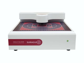
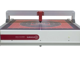
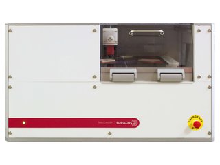
For wafer types Si, SiC, GaAs, GaN, glass, ceramic etc and for sizes 1” to 12”, SURAGUS’ full product portfolio includes manual single point tools, automated imaging tools and sensor integration kits for tool integration into existing or new tools.
 Sensor XS |
 Sensor S-SemiVac |
 Sensor S |
 Sensor M |
For product requests contact us by using the