

For product requests contact us by using the
- Contact formular,
- Email (sales@suragus.com) or
- Phone (+49 351 32 111 520).
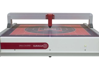
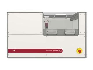
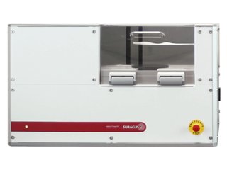
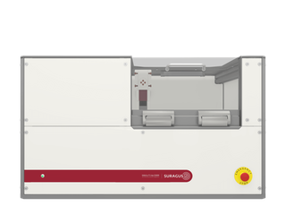
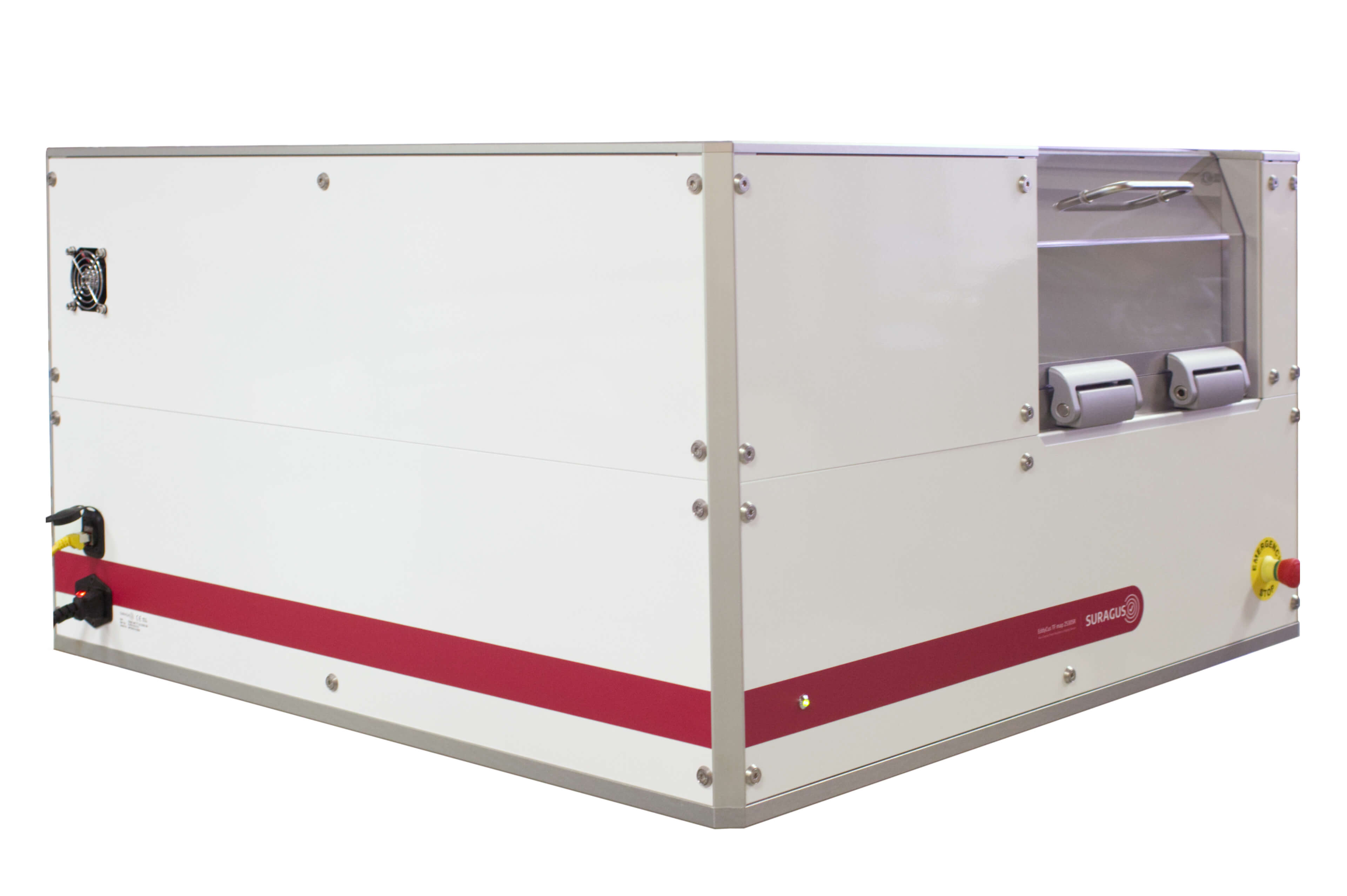
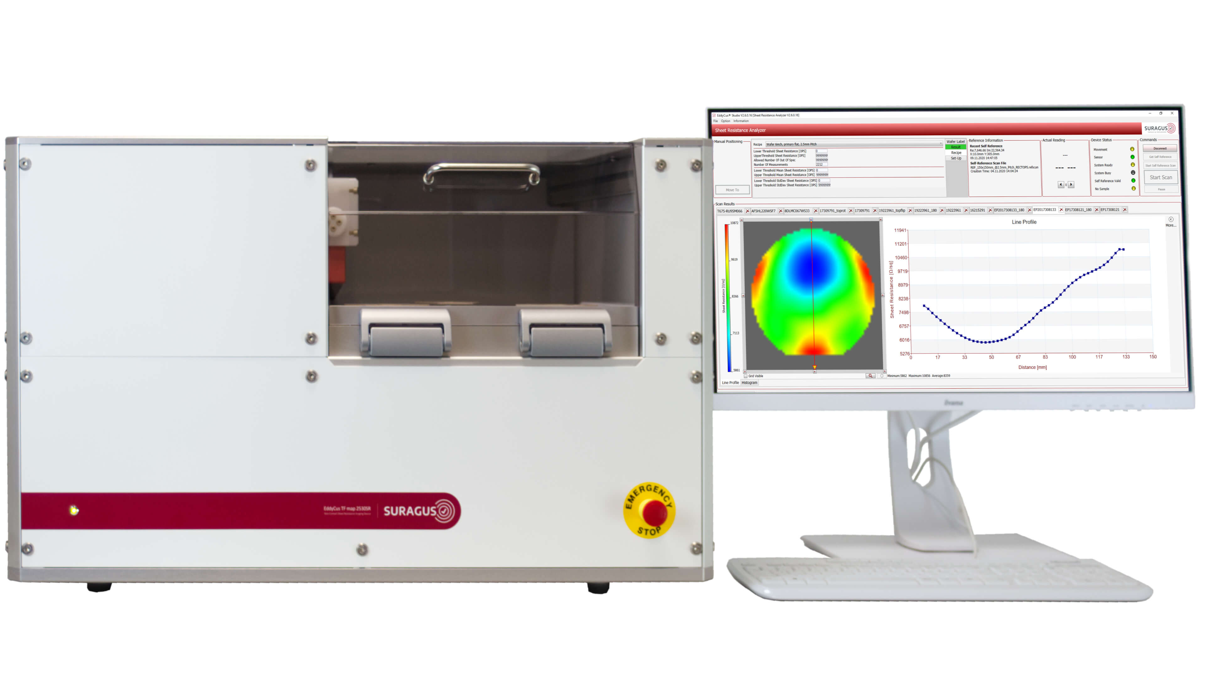
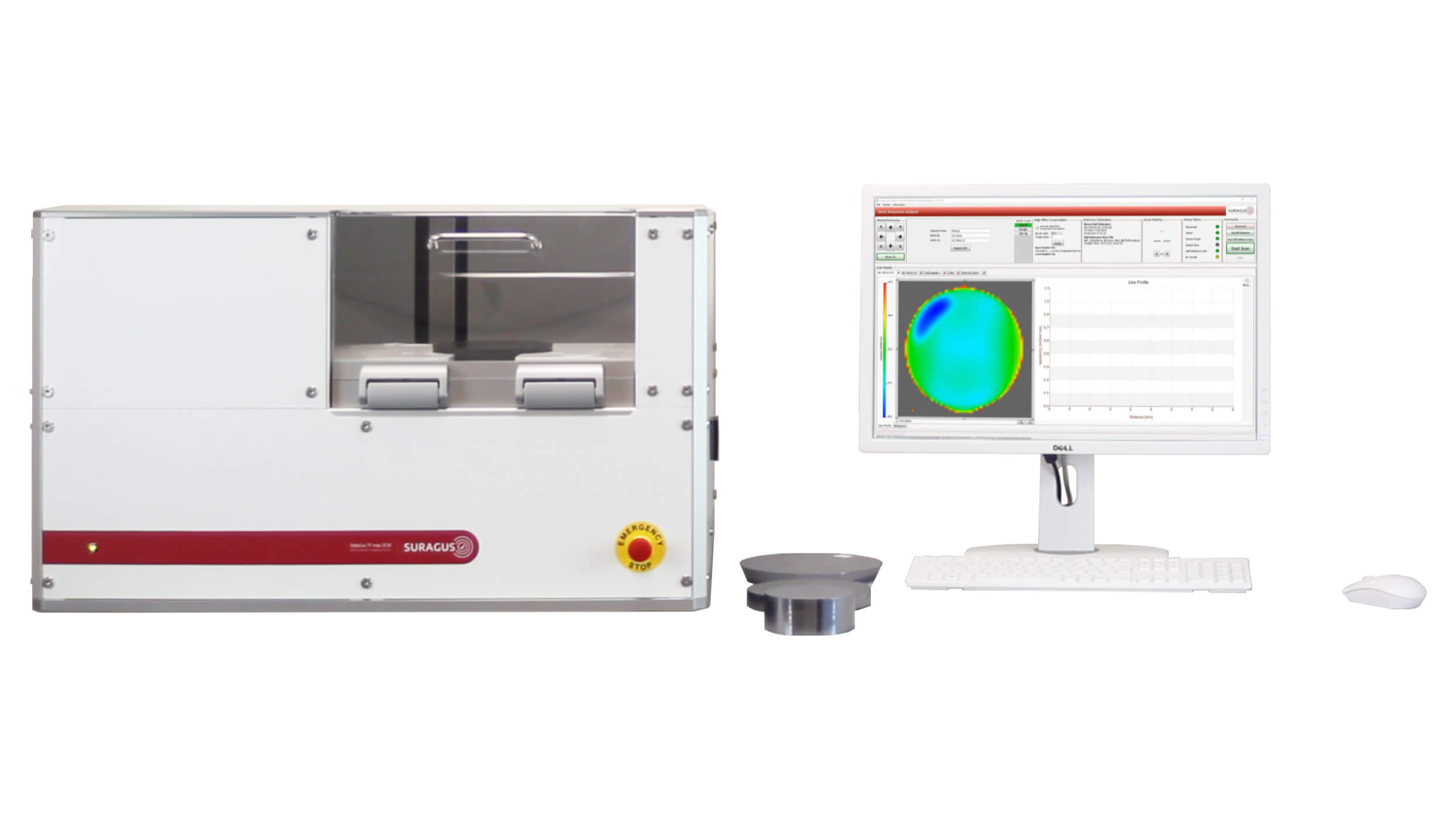
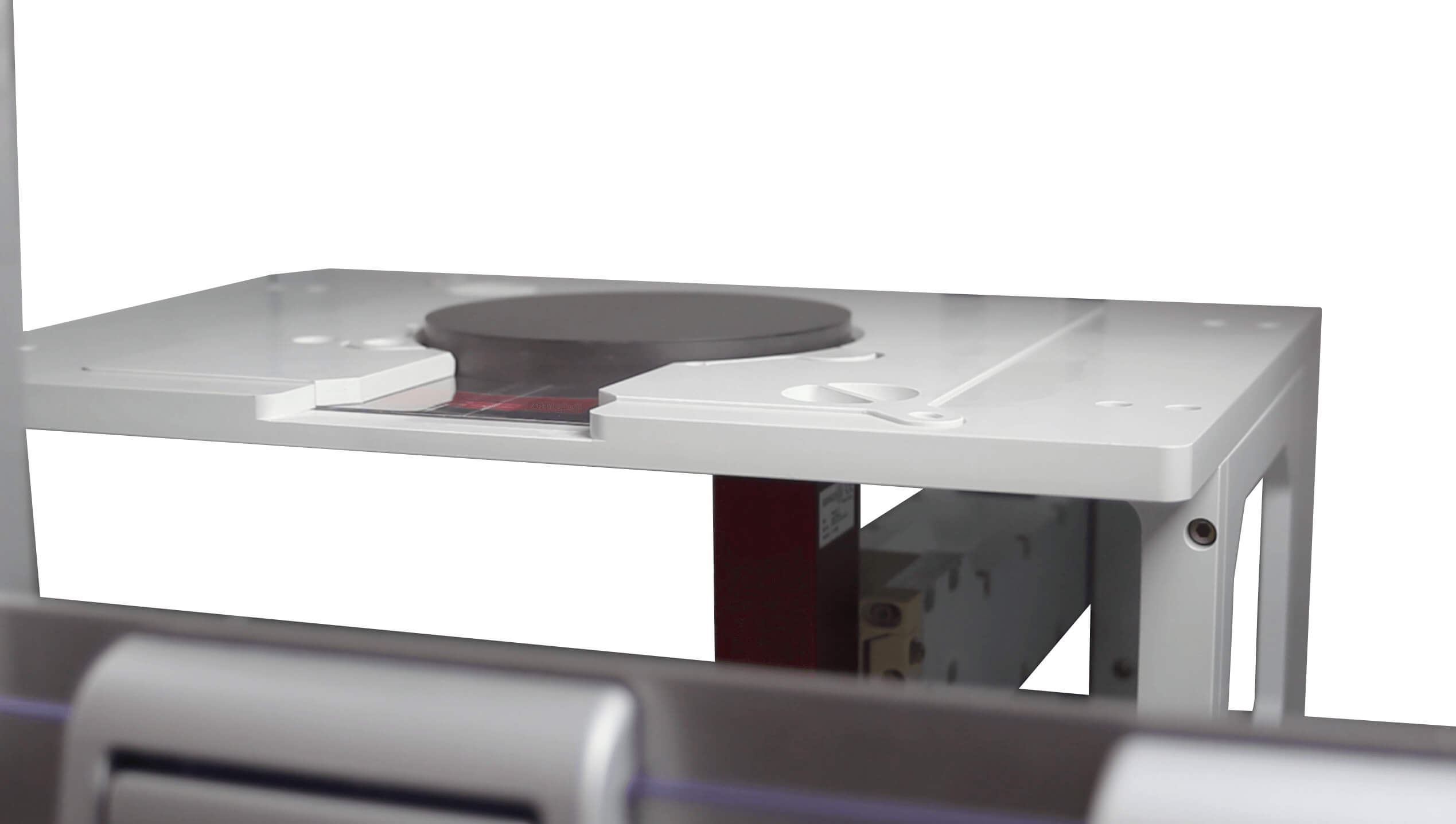
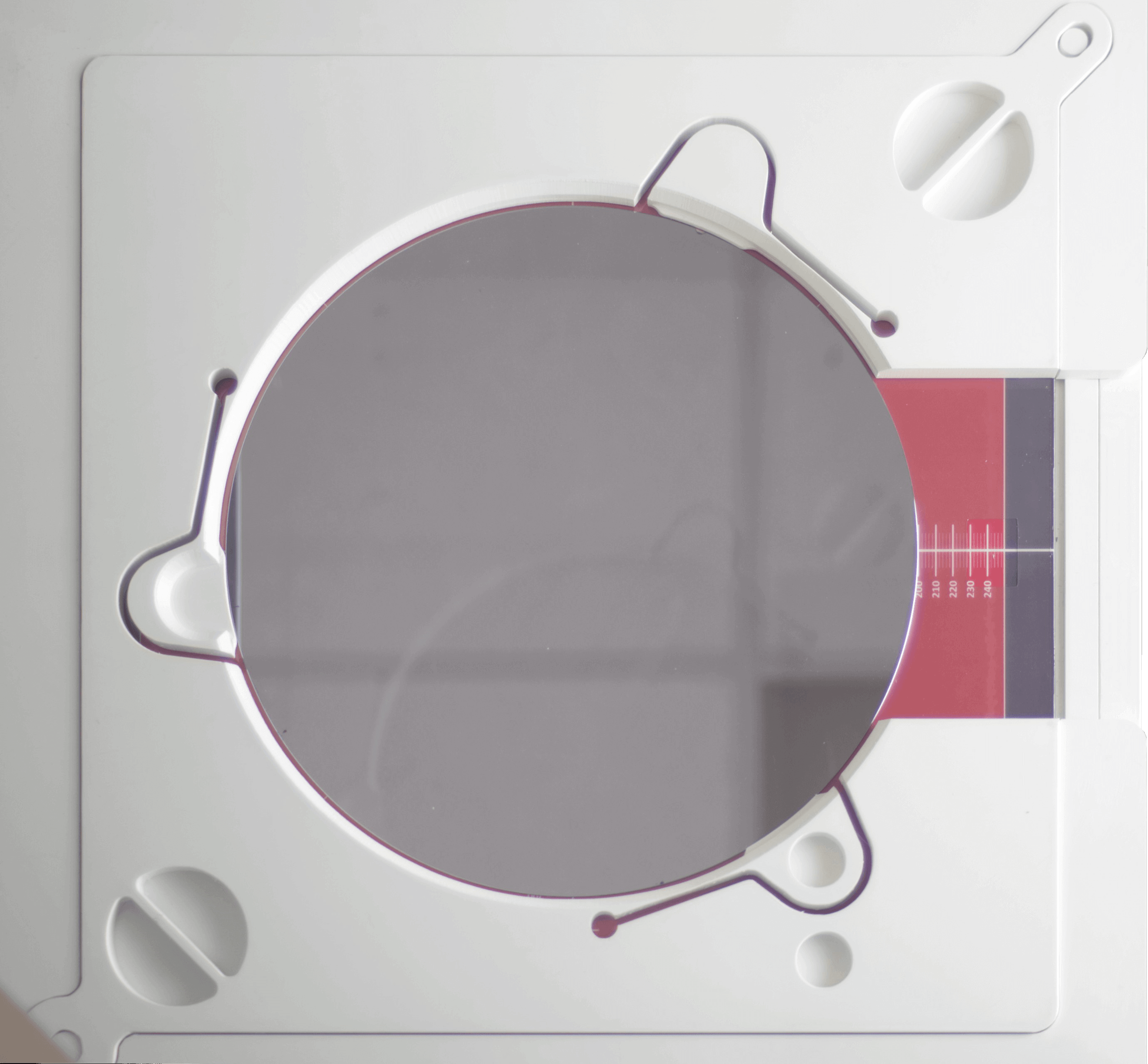
The EddyCus® map 2530 Series automatically measures the sheet resistance of large samples up to 300 x 300 mm² (12 x 12 inches) in non-contact mode. Upon manual sample positioning the device automatically measures and displays an accurate mapping of the sheet resistance across the entire sample area. The measurement settings allow easily and flexibly to choose between fast measurement times of below 1 minute or high spatial measurement resolution of more than 100,000 measurement points.
The device platform is available in different sensor configurations including eddy current sensors for electrical characterization or sensors for optical characterization. Variants of the measurement configurations involve the following options.
Combinations of the above variants are available as well (e.g. 2530SR-MT).
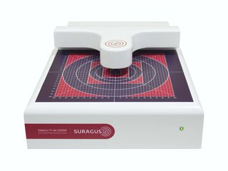
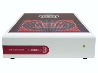
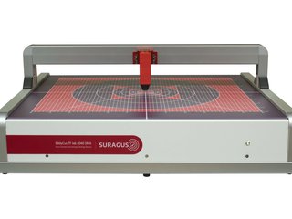
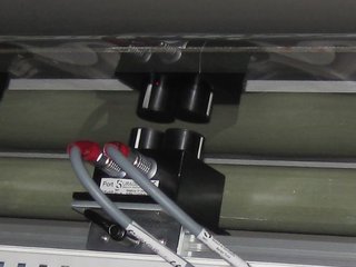
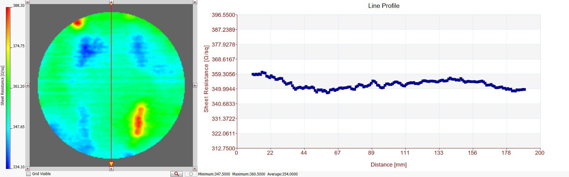
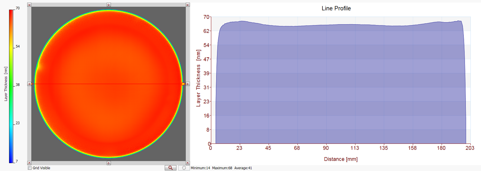
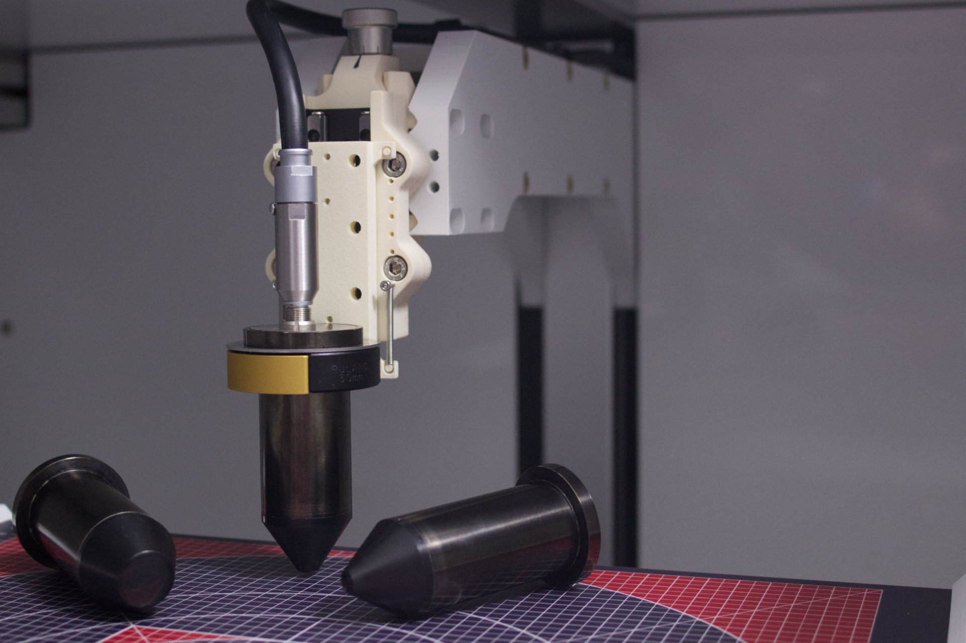
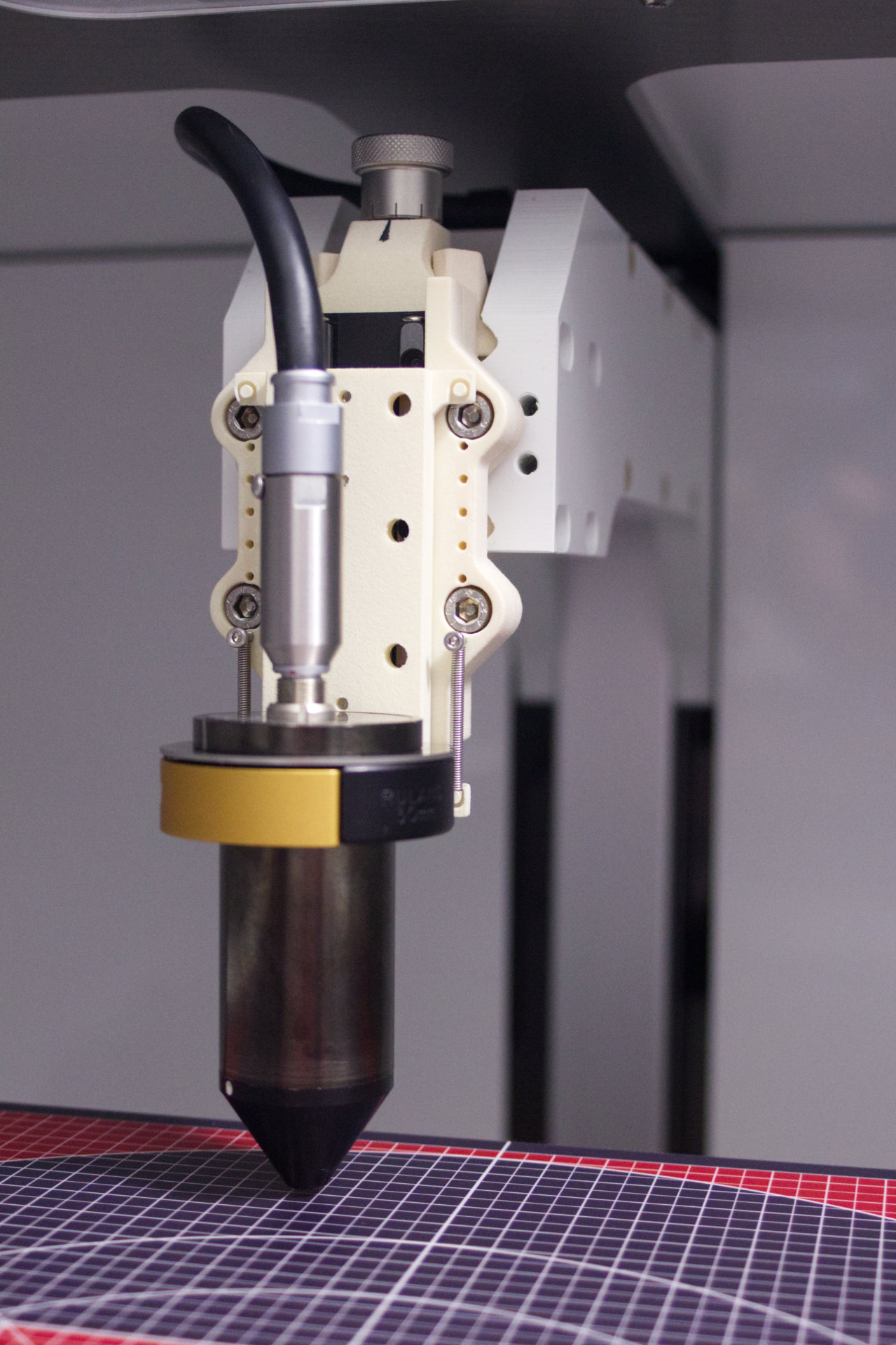
The EddyCus® map 2530 SR is a non-contact sheet resistance mapping system. The tool is equipped with a stationary Eddy Current sensor that measures the sheet resistance on up to 90,000 (300 x 300) measurements points per scan. The measurement stage holding the sample moves left and right with the stationary sensor taking measurements generating an image. Since this technology does not establish a physical contact with the specimen, the tool takes measurements on the fly. Additionally, it excels with high accuracies as it is independent of any contact quality. The quantity of measurement points taken across the sample enables the detection of multiple effects and defects. The measurement software comes with numerous options for advanced analysis of the measurement data. Furthermore, the comprehensive analysis features support a systematic quality assurance of various thin-films in manufacturing and R&D laboratories.
| Measurement technology | Non-contact eddy current sensor |
| Substrates | Wafer, glass, foils etc. |
| Max. scanning area | 12 inch / 300 mm x 300 mm (larger upon request) |
| Edge effect correction / exclusion | 2 – 10 mm (depending on size, range, setup and requirements) |
| Max. sample thickness / sensor gap | 3 / 5 / 10 / 15 mm (defined by the thickest sample) |
| Thickness measurement of metal films (e.g. aluminum, copper) | 2 nm – 2 mm (in accordance with sheet resistance ()) |
| Scanning pitch | 1 / 2.5 / 5 / 10 / 25 mm (other upon request) |
| Measurement points per time (square shaped samples) | 100 measurement points in 0.5 minutes 10,000 measurement points in 3 minutes |
| Scanning time | 8 inch / 200 mm x 200 mm in 1 to 10 minutes (1 – 10 mm pitch) 12 inch / 300 mm x 300 mm in 2 to 6 minutes (2.5 – 25 mm pitch) |
| Device dimensions (w/h/d) | 31.5” x 19.1” x 33.5” / 785 mm x 486 mm x 850 mm |
| Weight | 90 kg |
| Further available features | Metal thickness imaging, anisotropy and sheet resistance sensor |
| VLSR | LSR | MSR | HSR | VHSR | |
|---|---|---|---|---|---|
| 6 decades are measurable by one sensor, but with slightly affected accuracy | |||||
| Range [Ohm/sq] | 0.0001 – 0.1 | 0.1 – 10 | 0.1 – 100 | 10 – 2,000 | 1,000 – 200,000 |
| Accuracy / Bias | ± 1% | ± 1 – 3% | ± 3 – 5% | ||
| Repeatability (2σ) | < 0.5% | < 1% | < 0.5% | ||
| VLSR – Very Low Sheet Resistance , LSR – Low Sheet Resistance , MSR – Medium Sheet Resistance , HSR – High Sheet Resistance , VHSR – Very High Sheet Resistance | |||||
You are welcome to contact our team for
 |
 |
 |
 |
 |
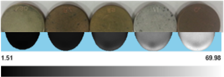
The EddyCus® map 2530 MT is a non-contact thickness imaging system that operates independent from any optical properties. The device utilizes a non-contact eddy current sensor to determine the thickness of any material with known conductivity or characteristic conductivity profile such as metals or alloys. This non-contact testing technology enables a precise measurement in a wide thickness range starting at a few nanometer thickness reaching up to millimeter range. Additionally, it can also be applied to films that are encapsulated by non-conductive materials. The measurement method is very robust and excels with a high repeatability and high accuracy. Its independency from the optical characteristics is beneficial for various industries that deposit non-transparent metal film. This compact benchtop system is used for a wide range of application for quick tests or systematic quality assurance in manufacturing R&D and testing laboratories.
| Measurement technology | Non-contact eddy current sensor |
| Substrates | Wafer, glass, foil, etc. |
| Max. scanning area | 12 inch / 300 mm x 300 mm (larger upon request) |
| Edge effect correction / exclusion | 2 – 10 mm (depending on size, range, setup and requirements) |
| Max. sample thickness / sensor gap | 3 / 5 / 10 / 25 mm (defined by the thickest sample) |
| Metal thickness range Accuracies depend on the selected setup and the type / conductivity of the metal (e.g. copper, aluminum, silver) |
Low 1 – 10 nm; 2 – 5 % accuracy Standard 10 – 1,000 nm; 1 – 3 % accuracy High 1 – 100 µm; 0.5 – 3 % accuracy |
| Metal thickness calibration | Direct thickness calibration / sheet resistance conversion |
| Sheet resistance range (optional) | 0.1 mOhm/sq – 100,000 Ohm/sq (in 5 ranges) |
| Scanning pitch (X and Y) | 1 / 2.5 / 5 / 10 / 25 mm |
| Scanning time | 8 inch / 200 mm x 200 mm in 1.5 to 15 minutes (1 – 10 mm pitch) 12 inch / 300 mm x 300 mm in 2 to 15 minutes (2.5 – 25 mm pitch) |
| Device dimensions (w/h/d) / weight | 31.5” x 19.1” x 33.5” / 785 mm x 486 mm x 850 mm / 90 kg |
| Further available features / other tool configurations | Sheet resistance measurement / conductivity / resistivity / anisotropy / permeability (beta) |
You are welcome to contact our team for
|
|
|
|
|
|
A variety of materials characteristics determine the conductivity of materials. Next to its composition also its structure and its purity affect the conductivity. The EddyCus® map 2530 RM is an eddy current mapping system dedicated to high-resolution imaging of conductivity and correlated characteristics exposing material properties, effects and defects. The system can be equipped with various EddyCus sensors for conductivity imaging in high resolution or high penetration and defect detection by use of differential probes. The system supports the creation of images (Eddy Current C-Scans) of the surface with a measurement pitch of 100 µm to 10 mm. The three axis systems is capable to scan 2D and 2.5D areas with a size of up to 300 x 300 mm / 12 x 12 inch. Typical applications cover the surface characterization of conductive materials such as SiC-, Graphite-, metal, alloy or steel plates or other conductive semi-finished products. Additionally, the system can be used for testing the electrical integrity of printed electronics and layers.
Eddy current testing allows the quantification of material conductivity [IACS or MS/m] or resistivity [Ohm·m]. The conductivity of materials provides information on material characteristics such as type of material and homogeneity of the material composition. Next to the direct information on electrical properties, the conductivity also contains information that relate to its thermic properties or its mechanical properties and its structural integrity.
| Measurement technology | High frequency eddy current sensor |
| Substrates | Flat, slightly curved |
| Max. scanning area | 8 inch / 220 mm x 220 mm x 10 mm |
| Edge effect correction / exclusion | 2 – 10 mm (depending on size, range, setup and requirements) |
| Max. sample thickness / sensor gap | 10 mm |
| Resistivity range | 0.002 – 0.1 mOhm cm 0.1 – 100 mOhm cm 100 – 1,000 mOhm cm |
| Conductivity range | 0.01 – 65 MS/m |
| Min. pitch | 0.1 mm |
| Mode | Contact and non-contact |
| Speed | 400 mm per second (time 1 to 30 minutes) |
| Device dimensions (w/h/d) | 31.5” x 19.1” x 33.5” / 785 mm x 486 mm x 850 mm |
| Weight | 90 kg |
| Further available features | Sheet resistance imaging, metal thickness imaging, anisotropy and sheet resistance sensor |
You are welcome to contact our team for
 |
|
 |
 |
 |
 |
 |
 |
 |
 |
 |
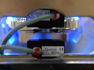
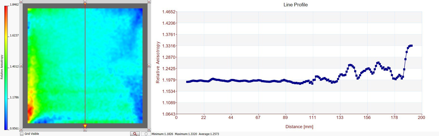
The EddyCus® map 2530 A (Anisotropy) is a unique anisotropy imaging system providing spatially resolved anisotropy images for profound understanding of the dominant orientation in wire structures. It utilized eddy current sensors that induce currents into defined directions. The resulting image shows the dominating wire direction, the anisotropy strength and the resulting sheet resistance. This unique tool is valuable for the characterization of wire structures such as Silver Nano Wires (Ag-NW), CNT, metal grids or nano-rod structures. Intentional anisotropic nanowires provide a better sheet resistance to optical transparency performance compared to isotropic nano-wire electrodes with opposite contact structure. This non-destructive testing method saves time and ensures that the wire deposition process provides the required orientation and resistance. This tool can be applied for quick quality checks or systematic quality assurance.
| Measurement technology | Non-contact eddy current sensor with directed current induction |
| Substrates | Foils, glass, wafer, etc. |
| Max. scanning area | 12 inch / 300 mm x 300 mm (larger upon request) |
| Max. sample thickness / sensor gap | 3 / 5 / 10 / 25 mm (defined by the thickest sample / application) |
| Sheet resistance range | 0.01 – 1,000 Ohm/sq; 1 to 5 % accuracy |
| Anisotropy range (TD/MD) | 0.33 – 3 (larger upon request) |
| Scanning pitch | 1 / 2.5 / 5 / 10 / 25 mm (other upon request) |
| Measurement points per time (square shaped samples) | 10,000 measurement points in 5 minutes 1,000,000 measurement points in 30 minutes |
| Scanning time | 8 inch / 200 mm x 200 mm in 1.5 to 15 minutes (1 – 10 mm pitch) 12 inch / 300 mm x 300 mm in 2 to 15 minutes (2.5 – 25 mm pitch) |
| Device dimensions (w/h/d) | 31.5” x 19.1” x 33.5” / 785 mm x 486 mm x 850 mm |
| Weight | 90 kg |
| Further available features | Metal thickness, sheet resistance, resistivity imaging |
You are welcome to contact our team for
|
|
|
|
|
|
The EddyCus® map 2530 HF is a high frequency eddy current mapping device designed for material and thin-film characterization. The device is sensitive to characteristics that correlate with electric, dielectric and magnetic properties. Typical applications include the assessment of material composition, the measurement of residual moisture, wet coating thickness or permittivity, and the determination of the content level of conductive (e.g. C, Pt) or magnetic (e.g. Co) materials. SURAGUS also supports complex impedance analysis to derive information on electrical, dielectric or magnetic properties from hybrid materials with a single measurement. The exact capabilities regarding specific measurement tasks can be provided from a consultation with the SURAGUS team.
| Measurement technology | Non-contact high frequency eddy current sensor |
| Substrates | Foils, glass, various containers |
| Max. scanning area | 12 inch / 300 mm x 300 mm (larger upon request) |
| Edge effect correction / exclusion | 2 – 10 mm (depending on size, range, setup and requirements) |
| Max. sample thickness / sensor gap | Transmission setup: 3 – 50 mm (defined by the thickest sample) Reflection setups: infinitive (only surface area is analyzed) |
|
Measurement types |
Wet thickness (µm) / weight (g/m²) / drying status (%) / conductivity (MS/m) / resistivity (mOhm cm) / permeabilty (H/m) Beta |
| Measurement range / accuracy | Depends on the measurement task and the material composition and test object volume. Please consult the SURAGUS team |
| Scanning pitch | 1 / 2.5 / 5 / 10 / 25 mm (other upon request) |
| Measurement points per time (square shaped samples) | 100 measurement points in 0.5 minutes 10,000 measurement points in 5 minutes 1,000,000 measurement points in 30 minutes |
| Device dimensions (w/h/d) | 31.5” x 19.1” x 33.5” / 785 mm x 486 mm x 850 mm |
| Weight | 90 kg |
| Further available measurements | Sheet resistance, metal thickness and anisotropy imaging |
You are welcome to contact our team for
|
|
|
|
|
|
For product requests contact us by using the