
.")


For product requests contact us by using the
- Contact formular,
- Email (sales@suragus.com) or
- Phone (+49 351 32 111 520).
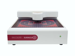
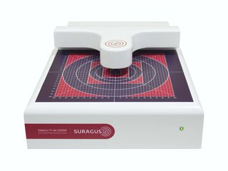
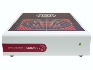
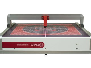
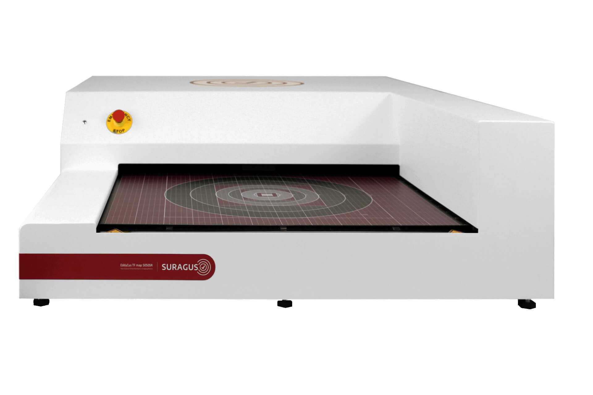
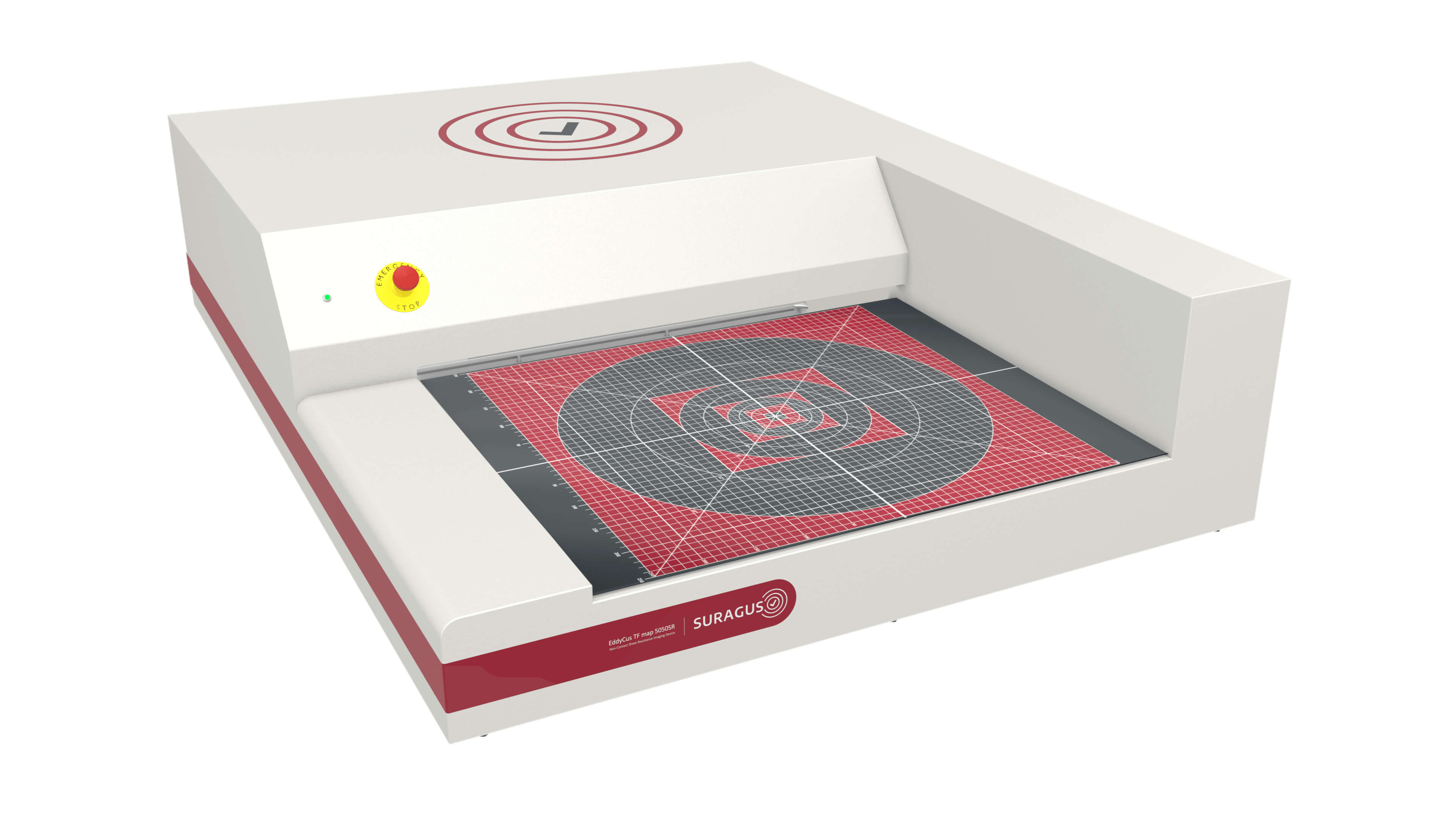
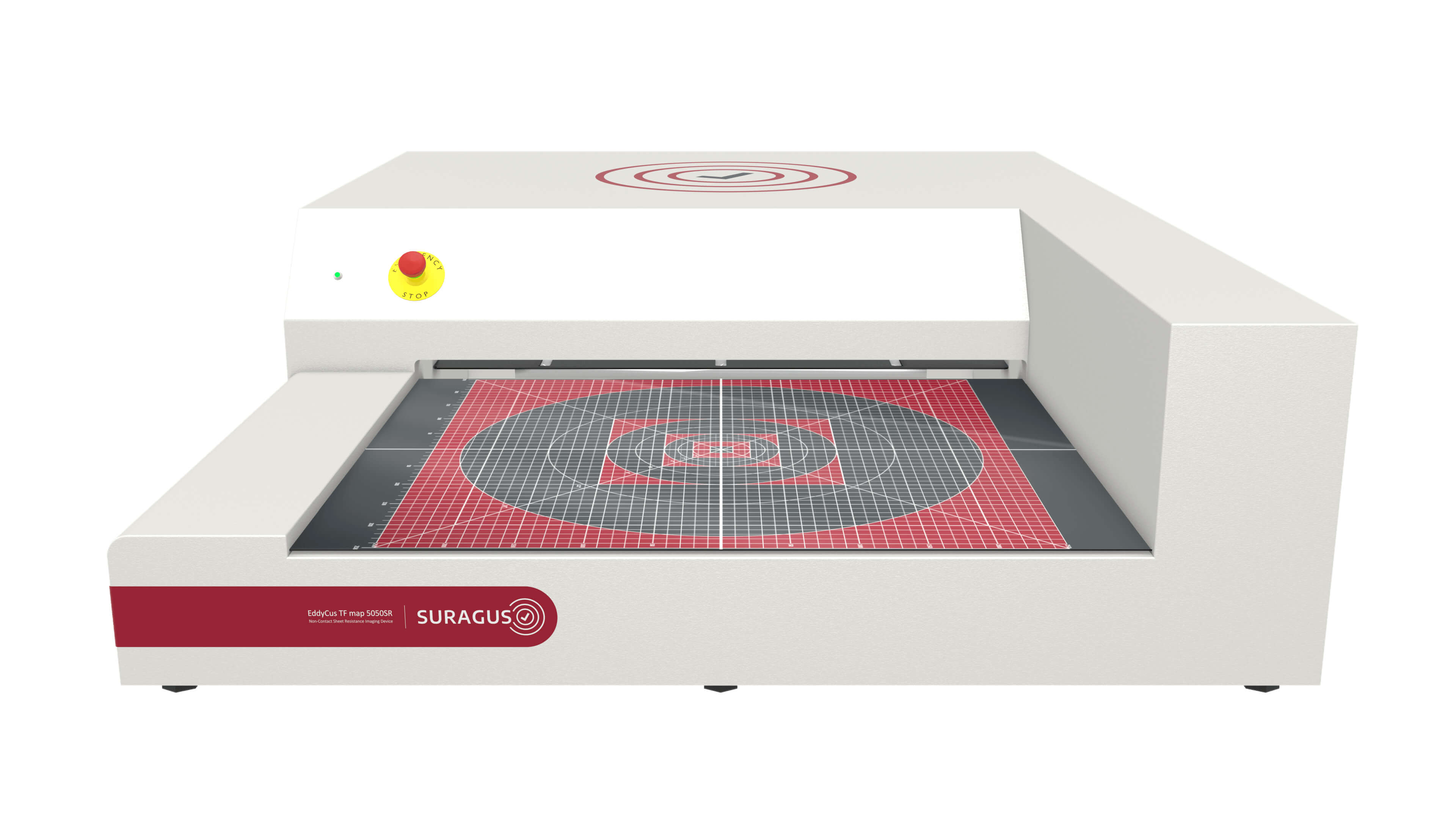
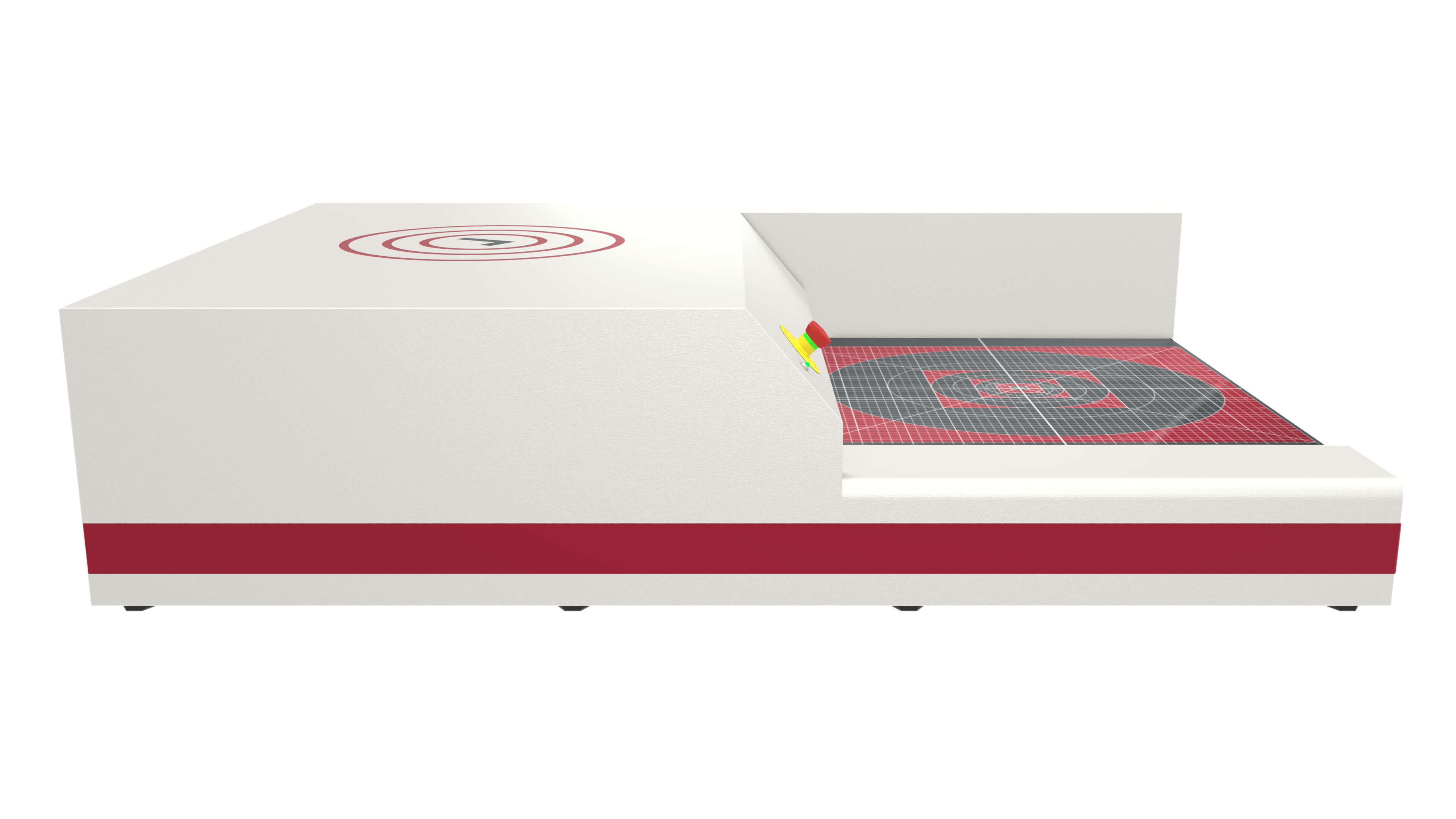
The EddyCus® TF map 5050 Series is a high-resolution non-contact imaging device series for sampling areas up to 500 x 500 mm (20 x 20 inch). The bench-top device automatically measures at various measurements points, typically with a pitch in X and Y of 1 mm (40 mil) generating accurate mappings. The system acquires hundreds of measurements per second on the fly resulting in high resolution images containing up to 250,000 measurement points per sample. The bench-top devices allow depending of its setup the precise imaging of metal thickness, sheet resistance or electrical anisotropy. The resulting property images provide a deep insight to layer homogeneity and defect density and hence offer a profound basis for material and process optimization. Applications involve quality assurance for sputtering, evaporation, ALD, CVD, electroplating or doping and annealing processes.
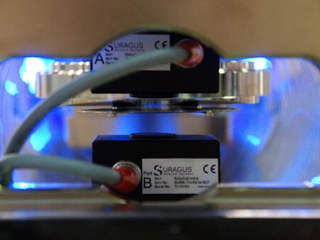
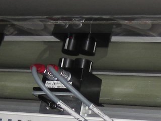
Devices are offered with different sensor configurations using eddy current sensors of optical components.
Combinations of the above variants are available as well (e.g. 5050SR-MT-A).
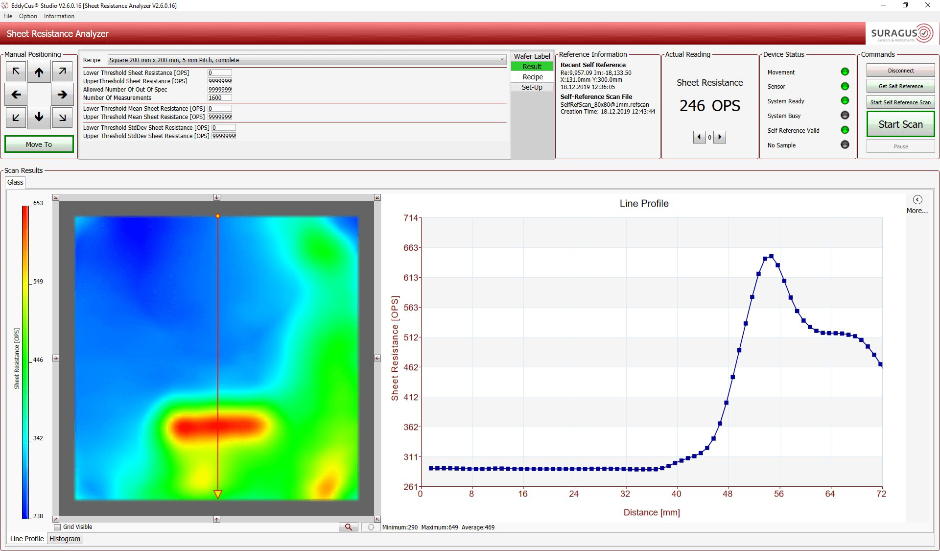
The EddyCus® TF map 5050SR is a non-contact sheet resistance imaging system. The system moves an eddy current sensor across the specimen. It measures on the fly the sheet resistance every 1 mm (40 mil) on up to 225.000 (500 x 500) measurements points per scan. The system excels with high accuracy since it operates independent from the contact quality. The resulting high-resolution images enable a confident assessment of the layer quality as this tool also exposes small defected areas. The software comprises easy to apply analysis features that involve statistics, reporting and exporting functions dedicated to systematic quality assurance.
| Measurement technology | Non-contact eddy current sensor |
| Substrates | 2 / 4 / 6 / 8 / 12 inch wafer |
| Max. scanning area | 20 inch / 508 mm x 508 mm (larger upon request) |
| Edge effect correction / exclusion | 2 – 10 mm (depending on size, range, setup and requirements) |
| Max. sample thickness / sensor gap | 3 / 5 / 10 / 15 mm (defined by the thickest sample) |
| Thickness measurement of metal films (e.g. aluminum, copper) | 2 nm – 2 mm (in accordance with sheet resistance ()) |
| Scanning pitch | 1 / 2 / 5 / 10 mm (other upon request) |
| Measurement points per time (square shaped samples) | 10,000 measurement points in 3 minutes 1,000,000 measurement points in 30 minutes |
| Scanning time | 8 inch / 200 mm x 200 mm in 0.6 to 6 minutes (1 – 10mm pitch) 12 inch / 300 mm x 300 mm in 0.9 to 9 minutes (1 – 10mm pitch) |
| Device dimensions (w/h/d) | 46.5“ x 11.4“ x 35.4“ / 1,180 mm x 290 mm x 900 mm |
| Weight | 120 kg |
| Further available features | Metal thickness imaging, anisotropy and sheet resistance sensor |
| VLSR | LSR | MSR | |
|---|---|---|---|
| 6 decades are measurable by one sensor, but with slightly affected accuracy | |||
| Range [Ohm/sq] | 0.0001 – 0.1 | 0.01 – 10 | 0.1 – 100 |
| Accuracy / Bias | ± 1% | ± 1 – 2% | ± 1 – 3% |
| Repeatability (2σ) | < 0.5% | < 1% | |
| VLSR – Very Low Sheet Resistance , LSR – Low Sheet Resistance , MSR – Medium Sheet Resistance | |||
You are welcome to contact our team for
 |
 |
 |
 |
 |
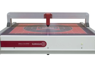
The EddyCus® TF map 5050MT is a high-resolution metal thickness imaging device. The device uses an eddy current sensor for precise non-contact thickness measurement. This electromagnetic measurement method is a contactless method that is able to measure through non-conductive covering layers as well. The measurements for the high-resolution thickness images are aggregated on the fly by automatically collecting hundreds of measurement at up to 250,000 positions across the sample. This measurement is independent from optical properties therefore it can also be well applied for thick non-transparent metal films. The measurement range is starting at a few nanometers reaching up to a few millimeter. The eddy current thickness measurement method is very fast and robust. It provides a very high repeatability and high accuracy. This advanced thickness meter is dedicated to quick thickness imaging or systematic quality assurance.
| Measurement technology | Non-contact eddy current sensor |
| Substrates | Wafer, glass, foil, etc. |
| Max. scanning area | 20 inch / 508 mm x 508 mm (larger on request) |
| Edge effect correction / exclusion | 2 – 10 mm (depending on size, range, setup and requirements) |
| Max. sample thickness / sensor gap | 3 / 5 / 10 / 15 / 25 mm (other upon request) |
| Metal thickness range Accuracies depend on the selected setup and the type / conductivity of the metal (e.g. copper, aluminum, silver) |
Low 1 – 10 nm; < 5 % accuracy Standard 10 – 1,000 nm; < 3 % accuracy High 1 – 100 µm; < 3 % accuracy |
| Metal thickness calibration | Direct thickness calibration / sheet resistance conversion |
| Sheet resistance range (optional) | 0.1 mOhm/sq – 100 Ohm/sq (in 5 ranges) |
| Parameter conversions | Sheet resistance, emissivity |
| Scanning pitch (x, y) | 1 / 2 / 5 / 10 mm (other on request) |
| Scanning time | 8 inch / 200 mm x 200 mm in 0.5 to 5 minutes (1 – 10mm pitch) 12 inch / 300 mm x 300 mm in 1.5 to 15 minutes (1 – 10mm pitch) |
| Device dimensions (w/h/d) / weight | 46.5“ x 11.4“ x 35.4“ / 1,180 mm x 290 mm x 900 mm / 120 kg |
| Further available features / other tool configurations | Sheet resistance measurement / conductivity / resistivity / anisotropy / permeability (beta) |
You are welcome to contact our team for
|
|
|
|
|
|
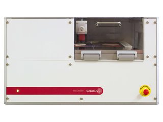
A variety of materials characteristics determine the conductivity of materials. Next to its composition also its structure and its purity affect the conductivity. The EddyCus® TF map 5050RM is an eddy current mapping system dedicated to high-resolution imaging of conductivity and correlated characteristics exposing material properties, effects and defects. The system can be equipped with various EddyCus sensors for conductivity imaging in high resolution or high penetration and defect detection by use of differential probes. The system supports the creation of images (Eddy Current C-Scans) of the surface with a measurement pitch of 100 µm to 10 mm. The three axis system is capable to scan 2D and 2.5D areas with a size of up to 500 x 500 mm / 20 x 20 inch. Typical applications cover the surface characterization of conductive materials such as SiC-, Graphite-, metal, alloy or steel plates or other conductive semi-finished products. Additionally, the system can be used for testing the electrical integrity of printed electronics and layers.
Eddy current testing allows the quantification of material conductivity [IACS or MS/m] or resistivity [Ohm m or Ohm / mm² / m]. The conductivity of materials provides information on material characteristics such as type of material and homogeneity of the material composition. Next to the direct information on electrical properties, the conductivity also contains information that relate to its thermic properties or its mechanical properties and its structural integrity.
Specification
Conductivity determination and conductivity imaging provides insights on:
| Measurement technology | High frequency eddy current sensor |
| Substrates | Flat, slightly curved |
| Materials | Wafer, boules, pucks, plates, thin film |
| Max. scanning area | 20 inch / 500 mm x 500 mm x 10 mm |
| Edge effect correction / exclusion | 2 – 10 mm (depending on size, range, setup and requirements) |
| Max. sample thickness / sensor gap | 3 / 5 / 10 / 25 mm (defined by the thickest sample) |
| Resistivity range accuracy can be optimized within a customer specified range |
0.002 – 0.1 mOhm cm 0.1 – 100 mOhm cm 100 – 1,000 mOhm cm |
| Sheet resistance range accuracy can be optimized within a customer specified range |
Low 0.0001 – 10 Ohm / sq; 2 – 5 % accuracy Standard 0.001 – 100 Ohm / sq; 2 – 5 % accuracy |
| Scanning pitch | 1 / 2 / 5 / 10 mm (other upon request) |
| Measurement points per time (square shaped samples) | 100 measurement points in 5 minutes 10,000 measurement points in 5 minutes |
| Scanning time | 8 inch / 200 mm x 200 mm in 0.5 to 5 minutes (1 – 10 mm pitch) 12 inch / 300 mm x 300 mm in 1.5 to 15 minutes (1 – 10 mm pitch) |
| Device dimensions (w/h/d) | 46.5” x 11.4” x 35.4” / 1,180 mm x 290 mm x 900 mm |
| Weight | 120 kg |
| Further available features | Metal thickness imaging, anisotropy and sheet resistance sensor |
You are welcome to contact our team for
|
|
|
|
|
|
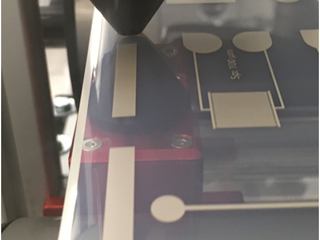
The EddyCus® TF map 5050A (Anisotropy) is a unique anisotropy imaging system providing spatially resolved anisotropy images for profound understanding of the dominant orientation in wire structures. It utilized eddy current sensors that induce currents into defined directions. The resulting image shows the dominating wire direction, the anisotropy strength and the resulting sheet resistance. This unique tool is valuable for the characterization of wire structures such as Silver Nano Wires (Ag-NW), CNT, metal grids or nano-rod structures. Intentional anisotropic nanowires provide a better sheet resistance to optical transparency performance compared to isotropic nano-wire electrodes with opposite contact structure. This non-destructive testing method saves time and ensures that the wire deposition process provides the required orientation and resistance. This tool can be applied for quick quality checks or systematic quality assurance.
| Measurement technology | Non-contact eddy current sensor with directed current induction |
| Substrates | Foils, glass, wafer, etc. |
| Max. scanning area | 20 inch / 508 mm x 508 mm (larger upon request) |
| Max. sample thickness / sensor gap | 3 / 5 / 10 / 25 mm (defined by the thickest sample / application) |
| Sheet resistance range | 0.01 – 100 Ohm/sq; 1 to 5 % accuracy |
| Anisotropy range (TD/MD) | 0.33 – 3 (larger upon request) |
| Scanning pitch | 1 / 2 / 5 / 10 mm (other upon request) |
| Measurement points per time (square shaped samples) | 10,000 measurement points in 5 minutes 1,000,000 measurement points in 30 minutes |
| Scanning time | 8 inch / 200 mm x 200 mm in 0.5 to 5 minutes (1 – 10mm pitch) 12 inch / 300 mm x 300 mm in 1.5 to 15 minutes (1 – 10mm pitch) |
| Device dimensions (w/h/d) | 46.5“ x 11.4“ x 35.4“ / 1,180 mm x 290 mm x 900 mm |
| Weight | 120 kg |
| Further available features | Metal thickness, sheet resistance, resistivity imaging |
You are welcome to contact our team for
|
|
|
|
|
|
For product requests contact us by using the